Single-fiber bidirectional multimode wavelength division multiplexing photoelectric conversion device and manufacturing method

A photoelectric conversion device and wavelength division multiplexing technology, which is applied in the field of information transmission, can solve the problems that photoelectric conversion transmitters cannot be arranged together in a relatively compact manner, reduce the manufacturing cost of TFT wavelength division multiplexing devices, and the volume cannot be satisfied. , to achieve good implementation convenience, avoid layout interference, and improve processing yield

Active Publication Date: 2022-03-25
耀芯电子(浙江)有限公司
View PDF13 Cites 0 Cited by
  • Summary
  • Abstract
  • Description
  • Claims
  • Application Information

AI Technical Summary

Problems solved by technology

[0005] In the direction of single-fiber bidirectional multimode wavelength division multiplexing, figure 1 One of the biggest problems in the TFT wavelength division multiplexing device with the structure shown is the positional interference between the photoelectric conversion receiver 112 and the photoelectric conversion transmitter, combined with the accompanying drawings figure 1 Schematic structure, due to the limitation of the position, the photoelectric conversion receiver 112 and the photoelectric conversion transmitter cannot be arranged together in a relatively compact manner. Therefore, in order to realize single-fiber bidirectional wavelength division multiplexing, two TFT wavelength division multiplexing devices need to be set They are respectively used for signal reception and signal transmission, which cannot meet the needs of micro-miniature devices in terms of volume; in addition, the number of components used in the two TFT wavelength division multiplexing devices is large, which is not conducive to reducing the TFT wavelength division multiplexing. Manufacturing cost of the device

Method used


Image

  • Single-fiber bidirectional multimode wavelength division multiplexing photoelectric conversion device and manufacturing method
  • Single-fiber bidirectional multimode wavelength division multiplexing photoelectric conversion device and manufacturing method
  • Single-fiber bidirectional multimode wavelength division multiplexing photoelectric conversion device and manufacturing method

Examples


Embodiment Construction

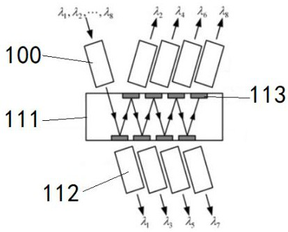
[0037] In order to make the purposes, technical solutions and advantages of the embodiments of the present application clearer, the following will clearly illustrate the spirit of the content disclosed in the application with the accompanying drawings and detailed descriptions. After any person skilled in the art understands the embodiments of the content of the application , when it can be changed and modified by the technology taught in the content of the application, it does not depart from the spirit and scope of the content of the application.

[0038] The exemplary embodiments and descriptions of the present application are used to explain the present application, but not to limit the present application. In addition, elements / members with the same or similar numbers used in the drawings and embodiments are used to represent the same or similar parts.

[0039] The terms "first", "second", ... etc. used herein do not specifically refer to a sequence or order, nor are they...


PUM


Abstract

The invention discloses a single-fiber bidirectional multimode wavelength division multiplexing photoelectric conversion device and a manufacturing method, and particularly relates to the technical field of information transmission, the device comprises a PCBA, and the PCBA comprises a circuit board, an optical splitter, a dielectric film filter, a laser and a photodiode; a conversion area is arranged on the circuit board; the area shape of the conversion area is an equilateral polygon, middle points of N + 1 edges of the equilateral polygon are sequentially connected according to the first turning direction to obtain an auxiliary polygon, and the auxiliary polygon is provided with N non-empty angles and an empty angle; a dielectric film filter is arranged on the non-empty corner; the laser and the photodiode are respectively arranged on two auxiliary extension lines penetrating through the dielectric film filter along a first rotating direction; and the optical splitter is arranged on an empty corner of the auxiliary polygon. The single-fiber bidirectional multimode wavelength division multiplexing photoelectric conversion device is based on a novel photoelectric bidirectional conversion structure constructed by a TFT (Thin Film Transistor), and a bidirectional wavelength division multiplexing function can be realized in a relatively compact volume.

Description

technical field [0001] The invention belongs to the technical field of information transmission, and in particular relates to a single-fiber bidirectional multi-mode wavelength division multiplexing photoelectric conversion device and a manufacturing method. Background technique [0002] With the increasing transmission capacity in the communication field, it is difficult for traditional transmission technology to meet the requirements of transmission capacity and transmission speed. Currently, data centers, business applications, and homes have higher and higher bandwidth requirements, and the applications are diverse. The photoelectric conversion device is the main component of the equipment to realize optical communication. In some applications, it is hoped that a single optical fiber can be used to achieve the same function. effective solution. [0003] Thin-film filter technology is the earliest wavelength-division multiplexing technology that has been applied since W...

Claims


Application Information

Patent Timeline
Patent Type & Authority Applications(China)
IPC IPC(8): G02B6/42
CPCG02B6/4215G02B6/428G02B6/4295G02B6/4296
Inventor 莫程智
Owner 耀芯电子(浙江)有限公司
Why Eureka
Try Eureka