
Backboard

A backplane and substrate substrate technology, which is applied to electrical components, electric solid-state devices, circuits, etc., can solve the problem of not being able to improve the width-to-length ratio of the drive transistor, and achieve the effect of large width-to-length ratio, improved driving capability, and compact layout

Pending Publication Date: 2022-03-29
BOE TECH GRP CO LTD
View PDF0 Cites 0 Cited by
  • Summary
  • Abstract
  • Description
  • Claims
  • Application Information

AI Technical Summary

Problems solved by technology

[0003] The main purpose of the present invention is to provide a backplane to solve the problem in the prior art that the width-to-length ratio of the drive transistor cannot be increased when the size of the pixel area occupied by the pixel structure in the backplane is small when making the backplane.

Method used


Image

  • Backboard
  • Backboard
  • Backboard

Examples


Embodiment Construction

[0029] The following will clearly and completely describe the technical solutions in the embodiments of the present invention with reference to the accompanying drawings in the embodiments of the present invention. Obviously, the described embodiments are only some, not all, embodiments of the present invention. Based on the embodiments of the present invention, all other embodiments obtained by persons of ordinary skill in the art without making creative efforts belong to the protection scope of the present invention.

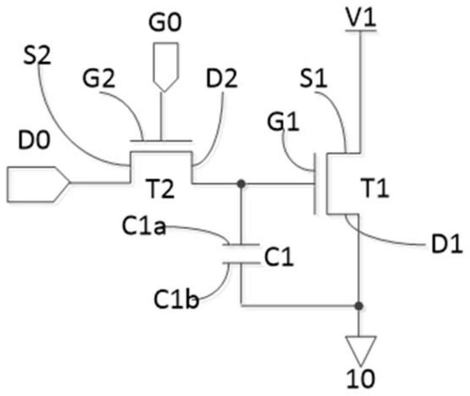
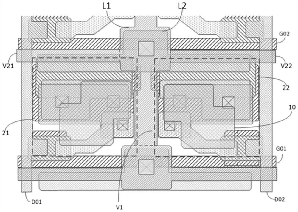
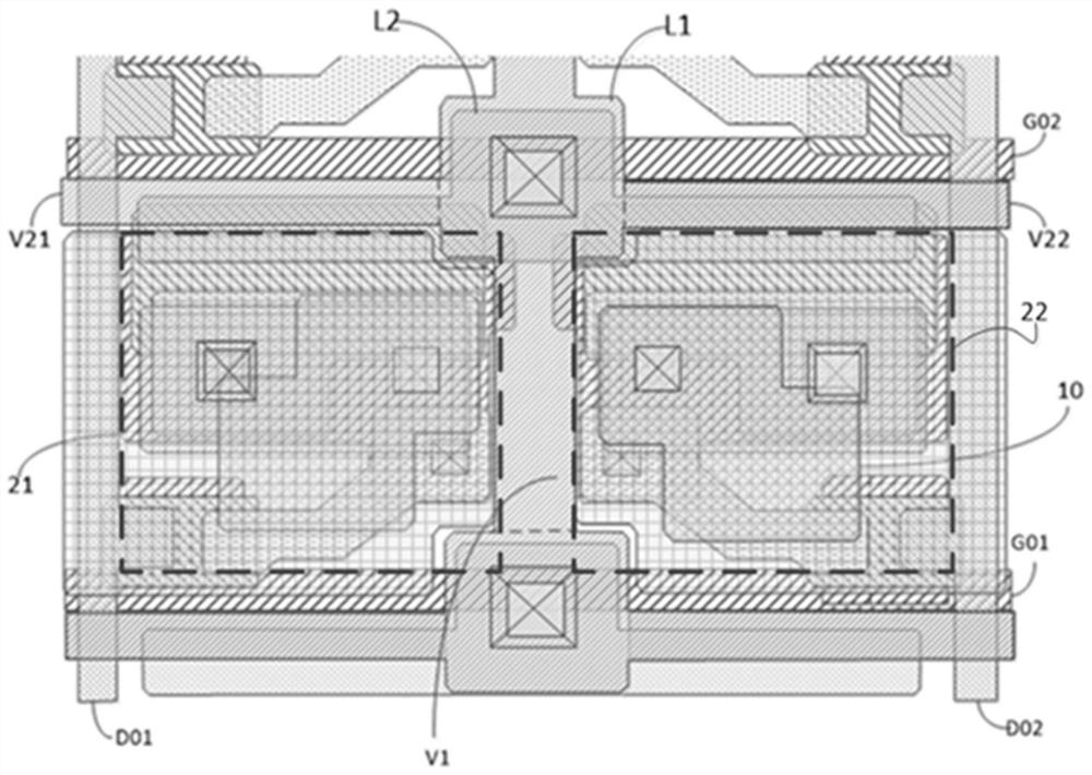
[0030] The backplane provided by the present application can at least be used as a printing backplane in a 3D printing system. The backplane contains printing anodes distributed in an array, and the backplane drives the anodes to realize 3D printing. Or the backplane provided by the present application can at least be used in the field of display to drive pixel electrodes (in this case, the anode of the backplane can be a pixel electrode, but not limited theret...


PUM


Abstract

The invention provides a back plate. The backboard comprises a substrate and pixel structures which are arranged on the substrate and are distributed in an array mode. The pixel structure comprises a power line, grid lines and data lines which are staggered in rows and columns, an anode of the back plate positioned on the substrate, a driving transistor electrically connected with the anode, and a switching transistor electrically connected with the driving transistor; the width direction of a channel in an active layer pattern of the driving transistor is the row direction, and the channel extends from a data line located on one side of the pixel structure to a power line located on the other side of the pixel structure in the row direction. According to the pixel structure provided by the invention, the area of the pixel structure can be reduced, and the width-to-length ratio of a TFT (Thin Film Transistor) is improved, so that the driving capability of a driving transistor is improved, and the resolution of a back plate is improved.

Description

technical field [0001] The present invention relates to the field of display technology or the field of 3D printing technology, in particular to a backplane. Background technique [0002] In the prior art, when making the backplane, when the size of the pixel area occupied by the pixel structure in the backplane is small, the driving transistors and switching transistors in the pixel structure cannot be rationally arranged, resulting in the inability to increase the aspect ratio of the driving transistors , the driving capability of the driving transistor cannot be improved. Contents of the invention [0003] The main purpose of the present invention is to provide a backplane to solve the problem in the prior art that the aspect ratio of the driving transistor cannot be increased when the size of the pixel area occupied by the pixel structure in the backplane is small when making the backplane. [0004] In order to achieve the above object, the present invention provides ...

Claims


Application Information

Patent Timeline
IPC IPC(8): H01L27/12H01L27/02
CPCH01L27/1222H01L27/124H01L27/1255H01L27/0207
Inventor 郭怡彤周健孙拓陈江博李延钊许晓春
Owner BOE TECH GRP CO LTD
Features
  • Generate Ideas
  • Intellectual Property
  • Life Sciences
  • Materials
  • Tech Scout
  • Unparalleled Data Quality
  • Higher Quality Content
  • 60% Fewer Hallucinations
Learn More