Fabricating fault tolerant non-linear waveguide cones

A nonlinear waveguide technology, applied in the design and manufacture of tapered waveguide, heterogeneous transition field, can solve the problem of increased light propagation loss and other issues

Pending Publication Date: 2022-04-01
OPENLIGHT PHOTONICS INC
View PDF0 Cites 0 Cited by
  • Summary
  • Abstract
  • Description
  • Claims
  • Application Information

AI Technical Summary

Problems solved by technology

Moreover, the light propagation loss in the body of the waveguide increases linearly with the length of

Method used


Image

  • Fabricating fault tolerant non-linear waveguide cones
  • Fabricating fault tolerant non-linear waveguide cones
  • Fabricating fault tolerant non-linear waveguide cones

Examples


Embodiment Construction

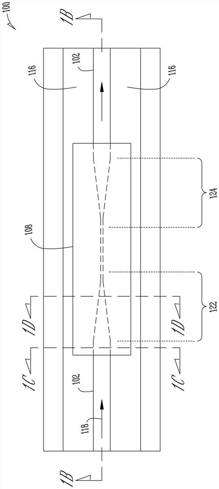
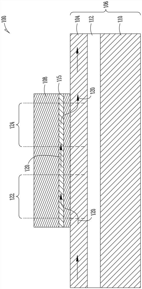
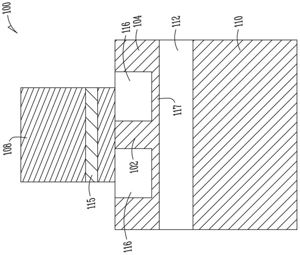
[0019] This paper describes a method for designing an optical waveguide transition with one or more nonlinear waveguide tapers that optimizes the trade-off between taper length and scattering loss. In a nonlinear waveguide cone, the cone profile (understood herein as the change in waveguide width as a function of length along the waveguide cone) is non-linear. For a given change in waveguide width with respect to a given cone length, a suitable nonlinear waveguide cone profile can achieve lower losses than a linear waveguide cone profile, or conversely, for a given limit on acceptable scattering losses, the nonlinear The waveguide cone can be designed shorter.

[0020] The precise cone profile for optimal performance depends on the scattering rate, which is a function of the waveguide width. The width-dependent scattering rate in turn depends on the design parameters of the waveguide transition, such as the fabricated dimensions (eg layer thickness) and material properties (e...


PUM


Abstract

A non-linear waveguide cone for manufacturing fault tolerance of waveguide transitions may be designed by: for each of a plurality of sets of parameter values characterizing the waveguide transitions (e.g., a set of nominal parameter values and a set of parameter values associated with a process corner representing a process variation from the nominal parameter values); calculating the scattering rate associated with the waveguide transition as a function of the waveguide width of the waveguide cone; determining an envelope of the calculated width dependent scatter; and calculating a non-linear cone profile of the waveguide cone based on the envelope. For the plurality of sets of parameter values, light propagation and coupling along the waveguide transition may be further computationally simulated to determine a minimum transmission value associated with the waveguide transition for a specified cone length, and/or to determine a minimum cone length at which the transmission value associated with the waveguide transition exceeds a specified threshold transmission value.

Description

technical field [0001] The present disclosure relates to optical waveguide transitions in photonic integrated circuits (PICs), eg, heterogeneous transitions between silicon waveguides and III-V waveguides. More particularly, the disclosed embodiments relate to the design and fabrication of tapered waveguides for low loss transitions. Background technique [0002] Silicon-based PICs benefit from low optical losses, ease of integration with electronic components, and manufacturability using standard photolithographic techniques. To allow the integration of active photonic devices, such as lasers, optical amplifiers, optical modulators, and photodetectors, into photonic circuits, III-V materials characterized by high electro-optic efficiency can be used in heterogeneous (sometimes called is "Hybrid") material platform combined with silicon. One conventional approach to achieve this heterogeneous material integration involves bonding a III-V die to a pre-patterned silicon-on-i...

Claims


Application Information

Patent Timeline
Patent Type & Authority Applications(China)
IPC IPC(8): G02B27/00G02B6/122
CPCG02B6/1228G02B6/12002G02B2006/12147G02B6/136G02B2006/12061
Inventor N·达尔凡德E·J·诺伯格
Owner OPENLIGHT PHOTONICS INC
Why Eureka
Try Eureka