

Method of fabricating optical non-linear thin film waveguide and optical nonlinear thin film waveguide
An optical nonlinear and thin-film waveguide technology, applied in nonlinear optics, optics, instruments, etc., can solve the problems of increased waveguide size and inability to obtain single-mode propagation
- Summary
- Abstract
- Description
- Claims
- Application Information
AI Technical Summary
Problems solved by technology
Method used
Image

Examples
Embodiment Construction
[0019] Preferred embodiments of the present invention will be described below with reference to the accompanying drawings.
[0020] [Structure of Optical Nonlinear Thin Film Waveguide]
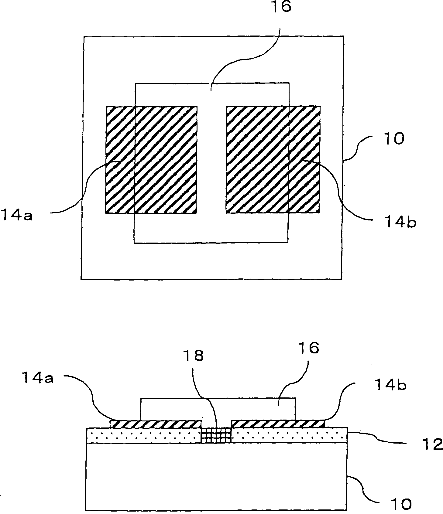
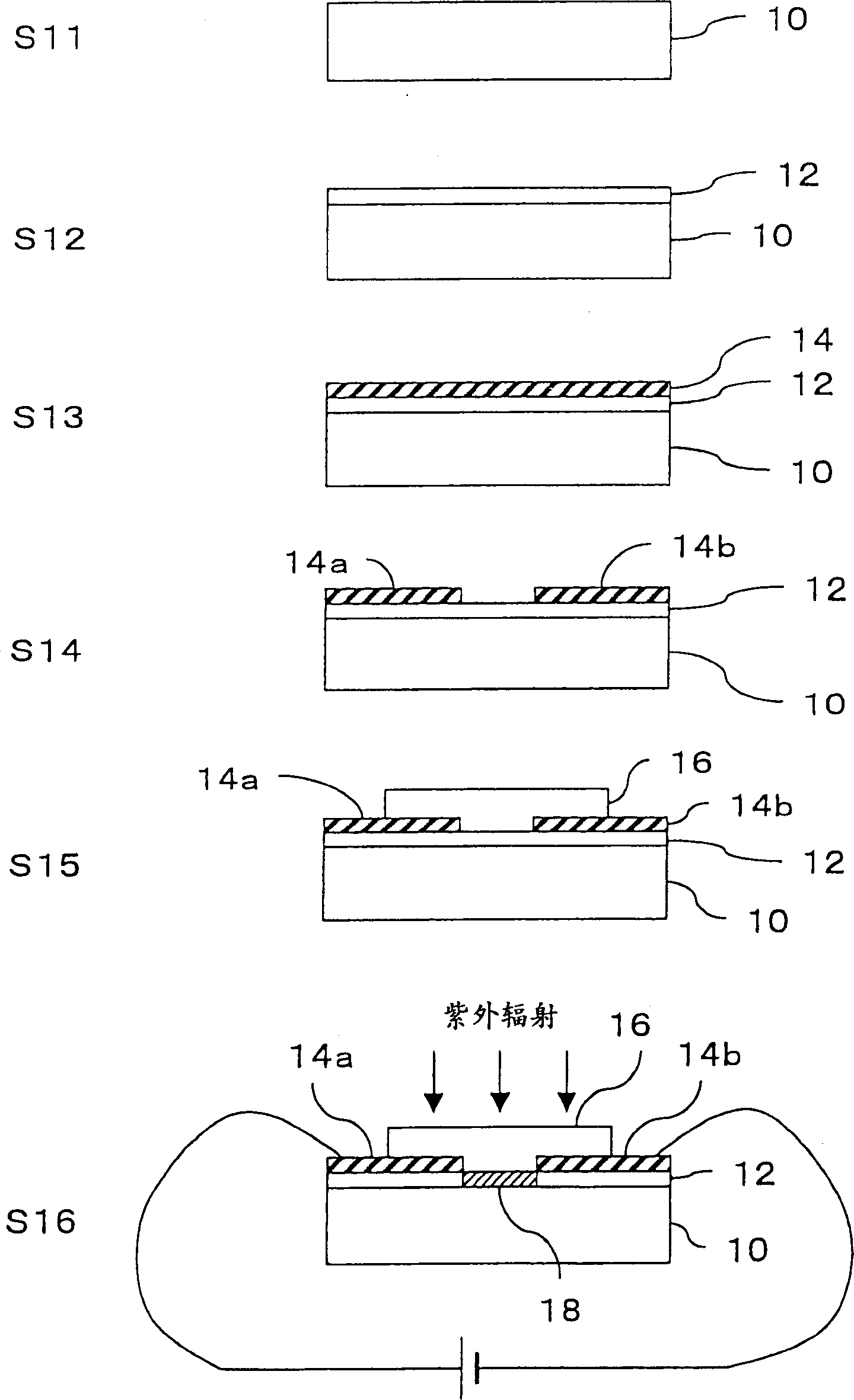
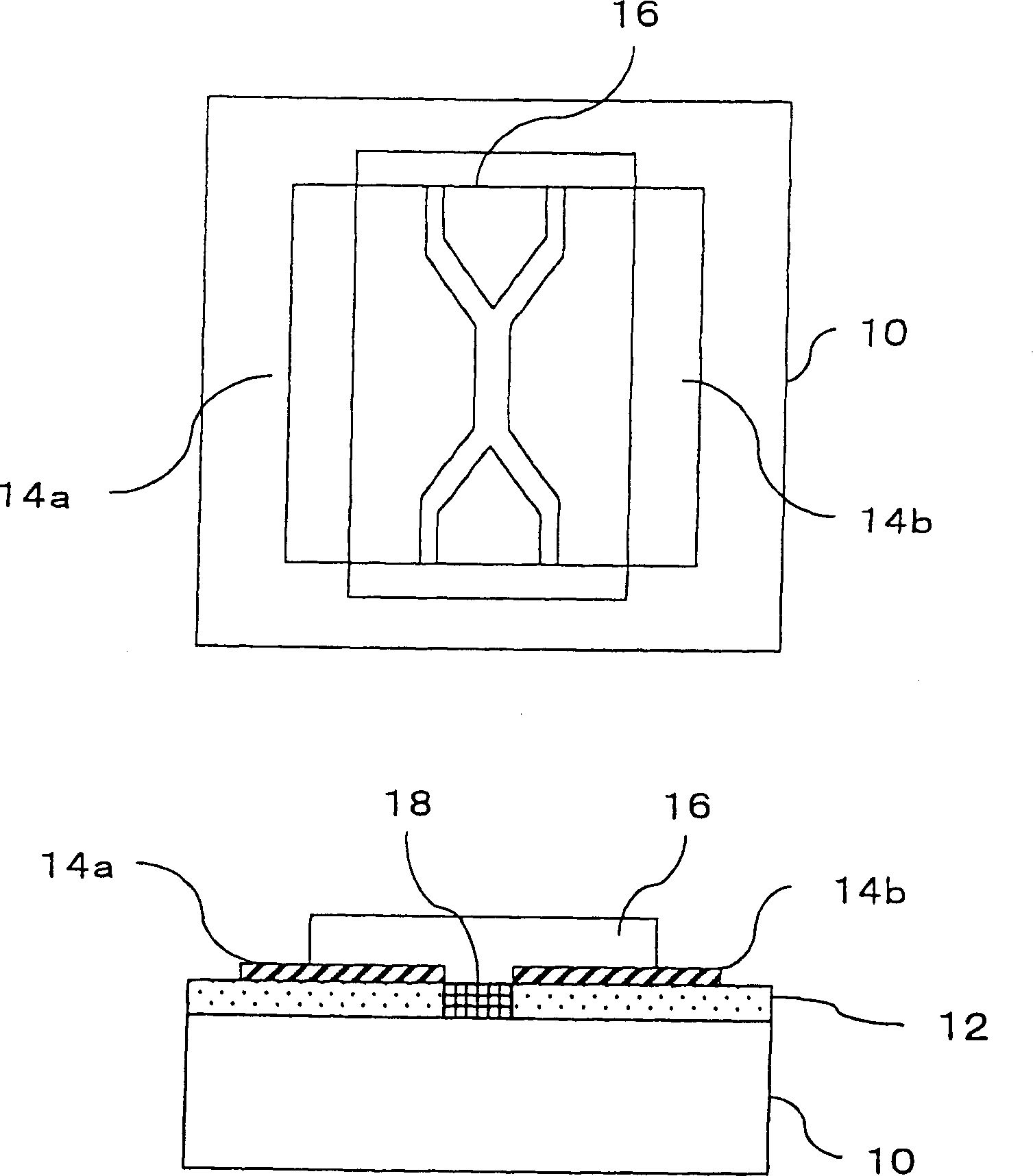
[0021] figure 1 The structure of the optical nonlinear thin-film waveguide (planar waveguide) according to the present invention is schematically shown. The glass substrate 10 is made of silica glass (SiO 2 glass) formed into flat sheets. Ge-doped SiO is formed on the surface of the substrate 2 Thin film 12, i.e. SiO containing Ge 2 The thickness of the thin film is about 1-5 μm, and the concentration of Ge is about 1-30% by mole. The specific value is determined according to the specifications of the planar waveguide, such as the wavelength to be used. Electrodes 14a and 14b are formed on SiO doped with Ge 2 On the film 12, prescribed pattern shapes are formed, and are opposed to each other with prescribed gaps therebetween. The electrodes 14a and 14b are formed of, for example, a thi...
PUM
| Property | Measurement | Unit |
|---|---|---|
| thickness | aaaaa | aaaaa |
Abstract
Description
Claims
Application Information