Device and method for realizing burning of multiple FPGAs based on CPLD chip

A chip and connector technology, applied in the field of FPGA chip programming, can solve the problems of limited driving capability of the drive source, affecting the programming speed, and programming failure, etc., to avoid damage to the FPGA chip, avoid stability degradation, and avoid PCB wiring. simple effect

Pending Publication Date: 2022-04-01
SUZHOU CENTEC COMM CO LTD
View PDF0 Cites 0 Cited by
  • Summary
  • Abstract
  • Description
  • Claims
  • Application Information

AI Technical Summary

Problems solved by technology

This method has the following disadvantages: (1) Due to the complexity of the daisy chain topology, the two signals TCK and TMS need to be connected to all FPGA chips in the daisy chain, and the discontinuity of the impedance on the signal link will cause signal reflection, thus affecting Signal integrity, signal overshoot, glitch, edge jitter, etc.
Moreover, once a signal integrity problem occurs, it will affect the signal rate at least, causing TCK frequency down to affect the programming speed, or directly lead to programming failure; (2) Due to the limited driving capability of the driving source, when the chips in the daisy chain exceed When there are more than 3, TCK and TMS need to add buffers to enhance the driving ability, which will increase the complexity of the circuit and the design cost; (3) Since the JTAG interface is directly connected to the FPGA chip, it is easy to damage when plugging and unplugging pin headers or EMI interference. The FPGA chip causes direct impact or damage; and if electrostatic breakdown occurs when plugging and unplugging, the damage to the FPGA is irreversible, resulting in increased costs; (4) When different FPGAs are programmed with different FPGA configurations, operational errors are prone to occur

Method used


Image

  • Device and method for realizing burning of multiple FPGAs based on CPLD chip
  • Device and method for realizing burning of multiple FPGAs based on CPLD chip
  • Device and method for realizing burning of multiple FPGAs based on CPLD chip

Examples


Embodiment Construction

[0023] The technical solutions of the embodiments of the present invention will be clearly and completely described below with reference to the accompanying drawings of the present invention.

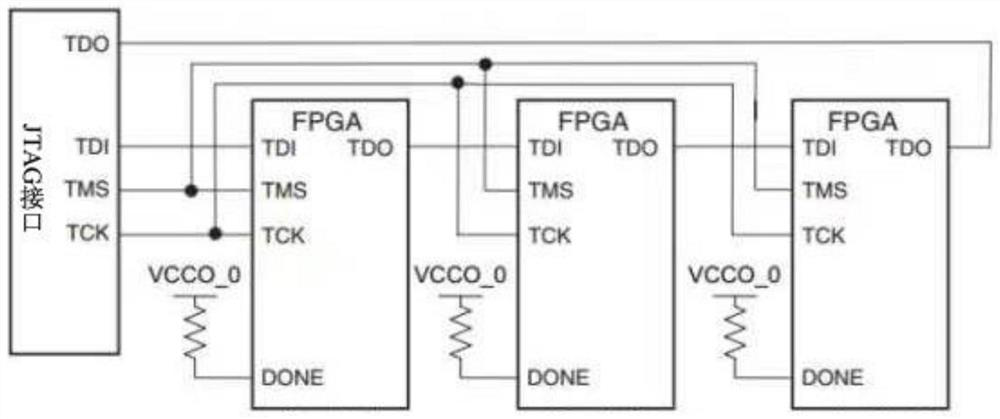
[0024] In the prior art, a plurality of FPGA chips are connected in a daisy chain (Dasiy Chain) form during programming, and this connection method not only easily affects the signal integrity, but also easily causes problems such as misoperation and damage to the FPGA chip. The present invention realizes the programming of multiple FPGA (Field-Programmable Gate Array, Field Programmable Gate Array) chips by adopting CPLD (Complex Programmable Logic Device) chips. Signal integrity, at the same time, can avoid damage and misoperation of the FPGA chip, and improve the stability of programming.

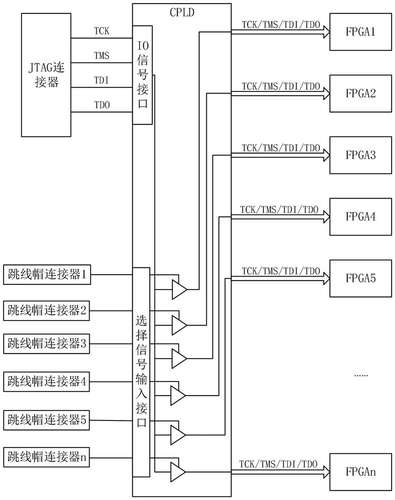
[0025] like figure 2 As shown, it is an apparatus for realizing programming of multiple FPGAs based on a CPLD chip disclosed in the present invention, including a JTAG (Joint Test Action Group, ...


PUM


Abstract

The invention discloses a device and method for achieving burning of multiple FPGAs based on a CPLD chip, the device comprises a JTAG connector and the CPLD chip, the JTAG connector is connected with an upper computer, the CPLD chip is connected with the JTAG connector and FPGA chips to be burnt, the CPLD chip is provided with a plurality of selection signal input interfaces, each selection signal input interface corresponds to one FPGA chip, and the selection signal input interfaces are connected with the JTAG connector and the FPGA chips to be burnt. And the CPLD chip controls the corresponding FPGA chip to be communicated with the JTAG connector according to a selection signal input by the selection signal input interface so as to burn the configuration file in the upper computer into the corresponding FPGA chip. The signal integrity can be ensured when the FPGA chip is burnt, meanwhile, damage and misoperation of the FPGA chip are avoided, and the burning stability is improved.

Description

technical field [0001] The invention relates to the technical field of FPGA chip programming, in particular to a device for realizing programming of multiple FPGAs based on a CPLD chip and a method for the device to realize programming of multiple FPGAs. Background technique [0002] FPGA (Field Programmable Gate Array, Field Programmable Gate Array) is a mainstream integrated circuit currently used on a large scale. Because of its reconfiguration property, that is, each IO signal interface on it can be configured and programmed according to actual needs, so compared with ASIC, it has the advantage of greater flexibility and can be widely used in chip emulation boards, network processing nodes and other scenarios middle. [0003] At present, the application of a single FPGA can no longer meet the needs of large-scale boards, and multiple FPGA chips need to be used. For example, multiple FPGA chips need to be used in scenarios such as chip emulation boards and network node b...

Claims


Application Information

Patent Timeline
Patent Type & Authority Applications(China)
IPC IPC(8): G06F8/61G06F13/40
Inventor 尚建力张志军卢增辉
Owner SUZHOU CENTEC COMM CO LTD
Why Eureka
Try Eureka