
A handling device, wafer processing equipment, and wafer concentricity adjustment method

A handling device and wafer technology, applied in the direction of transportation and packaging, semiconductor/solid-state device testing/measurement, electrical components, etc., can solve the problem of easily damaged support rings, affecting the separation of support rings, and it is difficult to ensure that the wafer and the debonding workbench Problems such as concentricity, to avoid damage and improve the effect of degumming

Active Publication Date: 2022-05-24
JIANGSU JCA ELECTRONICS TECH CO LTD
View PDF0 Cites 0 Cited by
  • Summary
  • Abstract
  • Description
  • Claims
  • Application Information

AI Technical Summary

Problems solved by technology

During the wafer handling process of the existing handling device, due to machine assembly errors or wear errors after long-term work, when the handling device places the ring-cut wafers on the debonding workbench, it is difficult to ensure that the wafers are completely bonded to the debonding workbench. The workbench is concentric, so that the UV film attached to the part of the circular cutting line and the support ring is blocked by the degumming workbench, and cannot receive the irradiation of the UV lamp, and the degumming cannot be realized, which reduces the degumming effect on the support ring and affects the follow-up Separate the support ring on the UV film, and it is easy to damage the support ring during the process of separating the support ring

Method used


Image

  • A handling device, wafer processing equipment, and wafer concentricity adjustment method
  • A handling device, wafer processing equipment, and wafer concentricity adjustment method
  • A handling device, wafer processing equipment, and wafer concentricity adjustment method

Examples


Embodiment Construction

[0045] In order to make the technical problems solved by the present invention, the technical solutions adopted and the technical effects achieved more clearly, the technical solutions of the present invention are further described below with reference to the accompanying drawings and through specific embodiments.

[0046] In the description of the present invention, unless otherwise expressly specified and limited, the terms "connected", "connected" and "fixed" should be understood in a broad sense, for example, it may be a fixed connection, a detachable connection, or an integrated ; It can be a mechanical connection or an electrical connection; it can be a direct connection or an indirect connection through an intermediate medium, and it can be the internal connection of two elements or the interaction relationship between the two elements. For those of ordinary skill in the art, the specific meanings of the above terms in the present invention can be understood in specific ...


PUM


Abstract

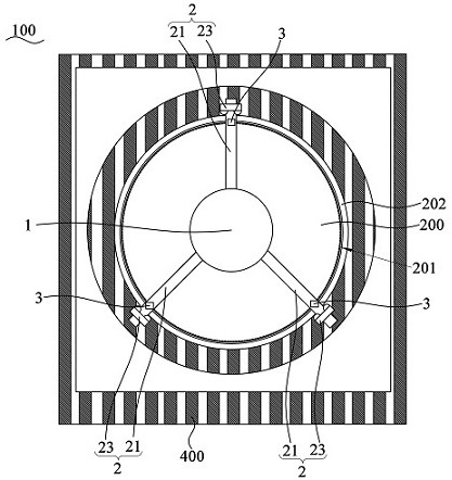
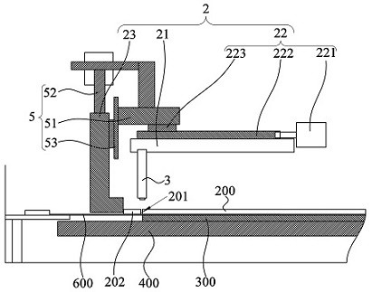
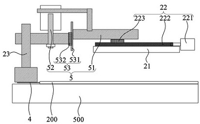
The invention relates to the technical field of semiconductor manufacturing, and relates to a handling device, wafer processing equipment and a wafer concentricity adjustment method. The handling device includes a handling component, multiple sets of energy detection components and multiple sets of centering adjustment components. The handling component can transport the ring-cut wafer from the upstream station to the disbonding workbench. The upper part is arranged at intervals in a circle with the disbonding workbench as the center of the circle. The circle surrounded by multiple sets of energy detection components is the same size as the circumference of the circular cutting line of the wafer. The energy detection components are used to detect the UV energy irradiated by the UV lamp. The centering adjustment components of the group are arranged at intervals around the wafer on the handling component. The centering adjustment components can push the wafer to move relative to the disbonding workbench, so that each energy detection component can detect UV energy and ensure that the wafer is in good contact with the wafer. Degumming workbench concentric. The wafer processing equipment and the wafer concentricity adjustment method apply the above-mentioned handling device to ensure the concentricity of the wafer and the debonding workbench.

Description

technical field [0001] The present invention relates to the technical field of semiconductor manufacturing, and in particular, to a conveying device, wafer processing equipment and a wafer concentricity adjustment method. Background technique [0002] In semiconductor manufacturing, wafers often need to be thinned to improve device performance. After the wafer is thinned, the support ring on the edge of the wafer needs to be cut and removed. The wafer thinning process includes the Taiko thinning process. The Taiko thinning process is to thin the middle area of ​​the wafer. The edge area of ​​the wafer is not thinned but acts as a support ring. After thinning, the support ring needs to be cut on the wafer, so that a circular dicing line is formed between the support ring and the wafer. Since the UV film is attached to the back of the wafer, the support ring will still adhere to the ring after being cut. On the UV film, it is necessary to use the handling device on the wafer ...

Claims


Application Information

Patent Timeline
Patent Type & Authority Patents(China)
IPC IPC(8): H01L21/66H01L21/677H01L21/68
Inventor 高阳葛凡张宁宁周鑫蔡国庆
Owner JIANGSU JCA ELECTRONICS TECH CO LTD
Learn More