Packaging structure and manufacturing method

A technology of packaging structure and packaging body, which is used in semiconductor/solid-state device manufacturing, semiconductor/solid-state device parts, semiconductor devices, etc., can solve the difficulty of balancing the thickness and hardness of the substrate, cannot meet the needs of high-density packaging, Laminated substrates cannot meet the problems of high-density packaging of electronic components, and achieve the effect of improving production yield, satisfying high density and small packaging volume.

Pending Publication Date: 2022-04-12
JCET GROUP CO LTD
View PDF0 Cites 0 Cited by
  • Summary
  • Abstract
  • Description
  • Claims
  • Application Information

AI Technical Summary

Problems solved by technology

The line width / line spacing of traditional laminated substrate wiring is usually around 15um / 15um, which is increasingly unable to meet the high-density packaging requirements of electronic components used in high-speed computing and artificial intelligence.
[0003] In addition, the traditional laminated substrate technology is 1) the supply of stacked dielectric materials; 2) the manufacturing cycle; 3) the wiring with a line width of less than 10um and the yield control of embedded chips; 4) the gap between substrate thickness and hardness There are great difficulties in balance and other aspects
[0004] Therefore, it is necessary to propose a new packaging structure and preparation method to overcome the traditional laminated substrate due to factors such as thickness, line width and line spacing, which cannot meet the needs of high-density packaging for electronic components used in high-speed computing and artificial intelligence.

Method used


Image

  • Packaging structure and manufacturing method
  • Packaging structure and manufacturing method
  • Packaging structure and manufacturing method

Examples


Embodiment Construction

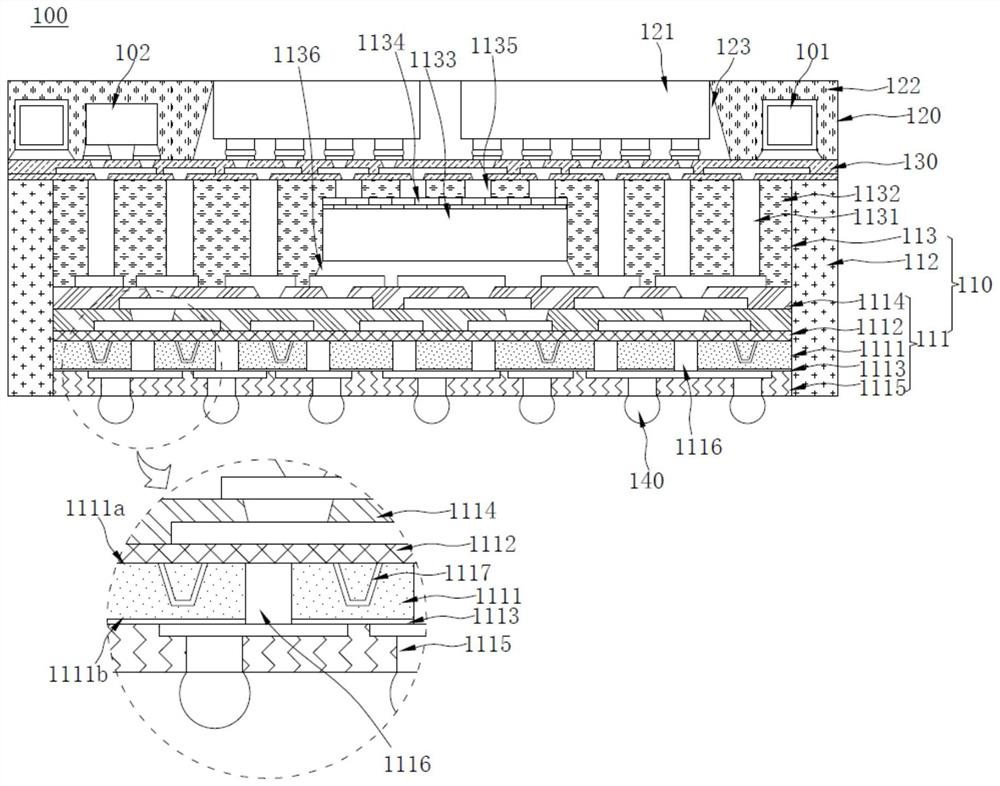
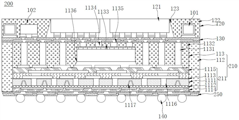
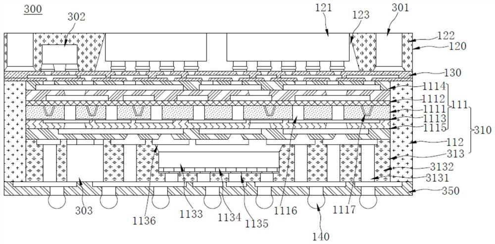
[0061] In order to make the object, technical solution and advantages of the present invention clearer, the present invention will be further described in detail below in conjunction with the embodiments and accompanying drawings. It should be understood that the specific embodiments described here are only used to explain the present invention, not to limit the present invention.

[0062] In the description of the present invention, it should be noted that the terms "center", "upper", "lower", "left", "right", "vertical", "horizontal", "inner", "outer" etc. The indicated orientation or positional relationship is based on the orientation or positional relationship shown in the drawings, and is only for the convenience of describing the present invention and simplifying the description, rather than indicating or implying that the referred device or element must have a specific orientation, or in a specific orientation. construction and operation, therefore, should not be constr...


PUM


Abstract

The invention provides a packaging structure and a manufacturing method. The packaging structure comprises a lower packaging body and an upper packaging body which are electrically connected, the lower packaging body comprises a prefabricated interconnected silicon core stacking structure and a first plastic packaging layer surrounding the periphery of the prefabricated interconnected silicon core stacking structure; the prefabricated interconnected silicon core stacking structure comprises a silicon interconnection layer, and the silicon interconnection layer comprises a first surface and a second surface which are opposite to each other; a back-end rewiring stacking layer and a first prefabricated rewiring stacking layer are stacked on the first surface, and the back-end rewiring stacking layer is electrically connected with the first prefabricated rewiring stacking layer; a passivation layer is arranged on the second surface; the silicon interconnection layer comprises a silicon substrate and a plurality of first pre-conduction columns embedded in a plurality of silicon through holes in the silicon substrate, each first pre-conduction column comprises a first end and a second end which are opposite to each other, the first end is exposed from the first surface, and the second end is exposed from one side, far away from the second surface, of the passivation layer; the upper packaging body is arranged above the first prefabricated redistribution stacking layer and is electrically connected with the first prefabricated redistribution stacking layer.

Description

technical field [0001] The invention belongs to the technical field of semiconductor packaging, in particular to a packaging structure and a manufacturing method. Background technique [0002] The rapid development of high-speed computing and artificial intelligence has put forward higher requirements for the packaging of semiconductor chips and packages, especially for packaging substrates, which usually require packaging substrates to have narrower line width / line spacing, more Good voltage drop control. The line width / line spacing of traditional laminated substrate wiring is usually around 15um / 15um, which is increasingly unable to meet the high-density packaging requirements of electronic components used in high-speed computing and artificial intelligence. [0003] In addition, the traditional laminated substrate technology is 1) the supply of stacked dielectric materials; 2) the manufacturing cycle; 3) the wiring with a line width of less than 10um and the yield contro...

Claims


Application Information

Patent Timeline
Patent Type & Authority Applications(China)
IPC IPC(8): H01L25/18H01L23/31H01L21/56H01L23/488H01L21/60
CPCH01L2224/18H01L2224/73204H01L2224/16225H01L2224/32225H01L2924/18161H01L2225/1058H01L23/5389H01L2225/1035H01L2225/1041H01L2225/1023H01L25/50H01L24/24H01L24/32H01L23/147H01L23/49827H01L24/82H01L25/0652H01L23/49816H01L21/4857H01L2924/00H01L21/56H01L23/3128H01L23/49811H01L23/5383H01L23/5384H01L25/105
Inventor 林耀剑刘硕杨丹凤周青云徐晨何晨烨
Owner JCET GROUP CO LTD
Why Eureka
Try Eureka