Pixel-misplaced indium gallium arsenic linear array detector, detection method and indium gallium arsenic photosensitive chip

An indium gallium arsenic and detector technology, which is applied in the direction of photometry and radiation control devices using electric radiation detectors, can solve the problems of high missed detection rate, achieve the effect of improving image resolution and reducing the probability of missed detection

Pending Publication Date: 2022-04-15
无锡中科德芯感知科技有限公司
View PDF0 Cites 0 Cited by
  • Summary
  • Abstract
  • Description
  • Claims
  • Application Information

AI Technical Summary

Problems solved by technology

[0003] The technical problem to be solved by the present invention is to overcome the defects of high missed detection rate caused by the existence of a certain photosensitive gap

Method used


Image

  • Pixel-misplaced indium gallium arsenic linear array detector, detection method and indium gallium arsenic photosensitive chip
  • Pixel-misplaced indium gallium arsenic linear array detector, detection method and indium gallium arsenic photosensitive chip
  • Pixel-misplaced indium gallium arsenic linear array detector, detection method and indium gallium arsenic photosensitive chip

Examples


Embodiment 1

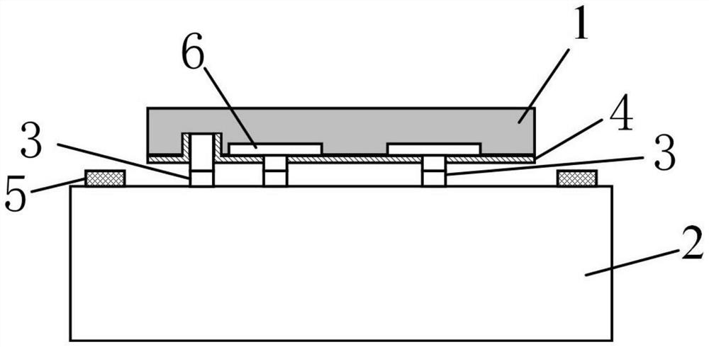
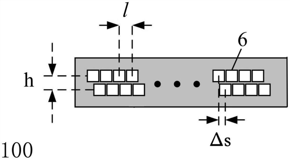
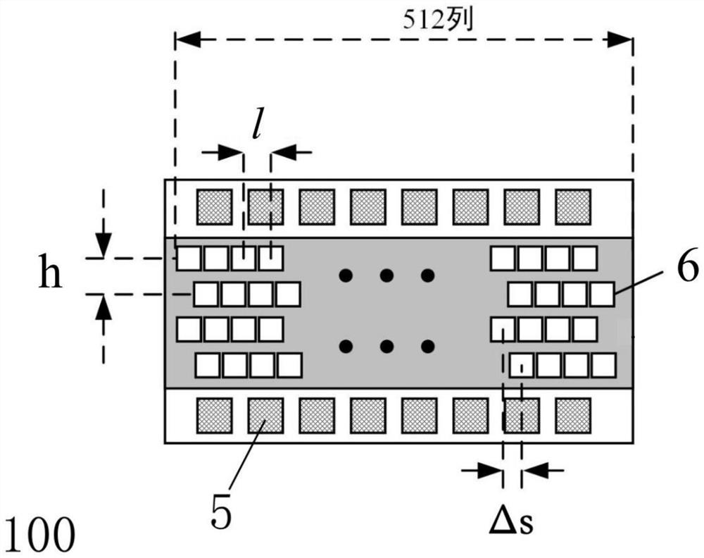
[0030] see figure 1 and 2 As shown, this embodiment specifically provides an InGaAs linear detector 100 with dislocated pixels. The InGaAs linear detector 100 includes an InGaAs photosensitive chip 1 . The InGaAs photosensitive chip 1 includes at least two rows of pixels of the same size arranged in parallel, and each pixel has a photosensitive area 6; the pixels in adjacent rows are staggered in the row direction. Since they are arranged in parallel, in the column direction, the projected length h of the center-to-center distance of any two pixels in different rows on the vertical plane is not less than the physical size of a single pixel in the column direction.

[0031] In this embodiment, an even-numbered pixel line column and an odd-numbered pixel line column are taken as an example for illustration. Since the pixels in these two lines and columns are misplaced along the row direction, the push-broom method In the process of detecting the same target in the imaging mode...

Embodiment 2

[0043] see Figure 5 As shown, this embodiment specifically provides a detection method based on an InGaAs linear detector, including steps:

[0044] S1. Push-broom imaging is performed on the detection object to obtain imaging data, and the imaging data is converted from pixel signals respectively obtained by the pixel elements of the InGaAs line detector.

[0045] S2. Determine abnormal values ​​in the pixel signal according to the threshold range.

[0046] S3. According to the abnormal value, it is determined that the position corresponding to the detection object and the pixel is an abnormal position.

[0047] For step S1 , the InGaAs linear detector 100 in Embodiment 1 may be used to perform push-broom scanning on the test object to obtain imaging data and comprehensively obtain relevant optical features of the test object. In a preferred manner, the pixel elements of each row and column of the InGaAs linear column detector 100 are arranged equidistantly along the row d...

Embodiment 3

[0052] This embodiment specifically provides an InGaAs photosensitive chip, which includes at least two rows of pixels of the same size arranged in parallel; and the pixels in adjacent rows are dislocated along the row direction.

[0053] As a preferred implementation manner, it may be the InGaAs photosensitive chip 1 in Example 1.

[0054] The InGaAs photosensitive chip of this embodiment forms a reasonable dislocation structure by setting pixels in two adjacent rows, and can effectively use the pixels in adjacent rows to achieve complementary imaging of the detection object, avoiding the The imaging gap does not respond to incident light, which significantly reduces the detection system's failure to detect abnormalities in the scene, and can improve the image resolution through image fusion processing, thereby improving the detection accuracy and expanding the application range.


PUM


Abstract

The invention discloses a pixel misplaced indium gallium arsenic linear array detector, a detection method and an indium gallium arsenic photosensitive chip. The indium gallium arsenic linear array detector comprises an indium gallium arsenic photosensitive chip, and the indium gallium arsenic photosensitive chip comprises at least two rows of pixels which are arranged in parallel. The pixels in adjacent rows are arranged in a staggered manner along the row direction; and the center distance between two adjacent rows of pixels in the column direction is not less than the physical size of one pixel in the column direction. According to the pixel staggered indium gallium arsenic linear array detector, the detection method based on the pixel staggered indium gallium arsenic linear array detector and the indium gallium arsenic photosensitive chip provided by the invention, a reasonable staggered structure is formed by two adjacent rows of pixels, so that the adjacent rows of pixels can be effectively utilized to realize imaging complementation of a detected object; the problem that an imaging gap of adjacent pixels has no response to incident light is avoided, the probability of missed detection of abnormity in a scene by a detection system is remarkably reduced, and the image resolution can be improved through image fusion processing.

Description

technical field [0001] The invention relates to the technical field of semiconductors, in particular to an indium gallium arsenic linear detector with dislocated pixels, a detection method and an indium gallium arsenic photosensitive chip. Background technique [0002] With the progress of science and technology and the development of society, the photoelectric detection system is developing towards higher resolution and smaller size, which requires the detector to have a larger scale and smaller center distance, so it is an ideal choice for short-wave infrared detection. InGaAs photosensitive chips usually have an array structure with back light incident. Compared with area array detectors suitable for staring imaging, linear array detectors are mainly used in push-broom imaging scenarios, such as airborne earth observation, industrial inspection, spectral analysis, grain screening, etc., and because of their lower cost Has a very broad market prospects. In order to reduc...

Claims


Application Information

Patent Timeline
IPC IPC(8): H01L27/144G01J1/42
Inventor 李雪刘大福顾溢孙夺
Owner 无锡中科德芯感知科技有限公司
Why Eureka
Try Eureka