LED chip die bonding method and LED panel

An LED chip and die-bonding technology, applied in electric solid devices, semiconductor devices, electrical components, etc., can solve the problem of high temperature resistance requirements of LED chips and array substrates, reduce the influence of thermal stress, reduce high temperature resistance requirements, The effect of flexible application degree

Pending Publication Date: 2022-04-29
TCL CHINA STAR OPTOELECTRONICS TECH CO LTD
View PDF0 Cites 1 Cited by
  • Summary
  • Abstract
  • Description
  • Claims
  • Application Information

AI Technical Summary

Problems solved by technology

[0004] Embodiments of the present invention provide a method for bonding LED chips and an LED panel to solve the problem that the existing method for bonding LED chips involves the high-temperature process of solder paste reflow rods, which leads to high-temperature performance requirements for LED chips and array substrates. high technical issues

Method used


Image

  • LED chip die bonding method and LED panel
  • LED chip die bonding method and LED panel
  • LED chip die bonding method and LED panel

Examples


Embodiment Construction

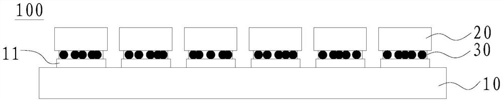
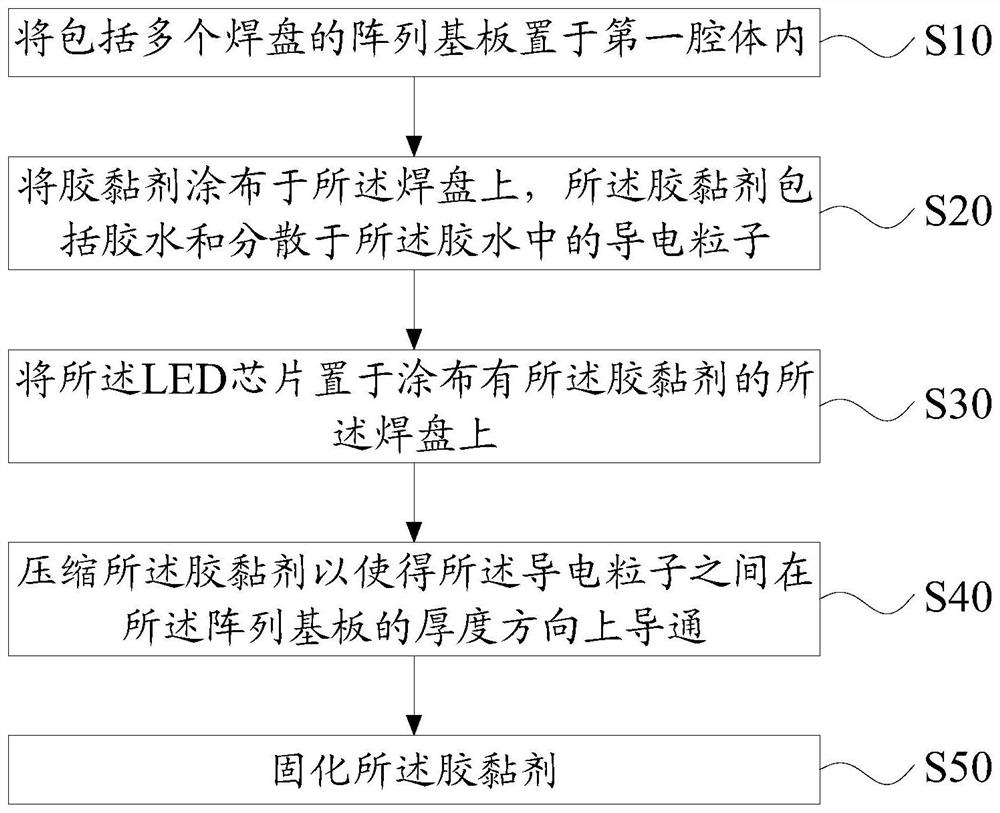
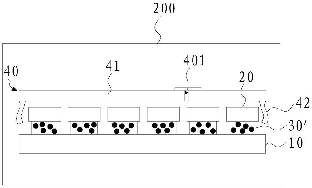
[0037] The technical solutions in the embodiments of the present application will be clearly and completely described below in conjunction with the drawings in the embodiments of the present application. Apparently, the described embodiments are only some of the embodiments of this application, not all of them. Based on the embodiments in this application, all other embodiments obtained by those skilled in the art without making creative efforts belong to the scope of protection of this application.

[0038] In the description of the present application, it should be understood that the orientation or positional relationship indicated by the terms "thickness", "upper", "lower", etc. is based on the orientation or positional relationship shown in the drawings, and is only for the convenience of describing the present application. and simplified descriptions, rather than indicating or implying that the device or element referred to must have a specific orientation, be constructe...


PUM

PropertyMeasurementUnit
Curing temperatureaaaaaaaaaa

Abstract

The embodiment of the invention discloses a die bonding method of an LED chip and an LED panel. The die bonding method comprises the following steps: S10, placing an array substrate comprising a plurality of bonding pads in a first cavity; s20, coating the bonding pad with an adhesive, wherein the adhesive comprises glue and conductive particles dispersed in the glue; s30, the LED chip is placed on the bonding pad coated with the adhesive; s40, compressing the adhesive to enable the conductive particles to be conducted in the thickness direction of the array substrate; and S50, curing the adhesive. According to the LED chip die bonding method provided by the embodiment of the invention, the conductive particles are dispersed in the glue to replace solder paste in the prior art to realize die bonding of the LED chip, so that on one hand, the high-temperature process of solder paste reflow soldering can be avoided, the high-temperature-resistant requirement on the LED chip and an array substrate selected material can be reduced, and the residual thermal stress influence of the high-temperature process can be reduced; on the other hand, different glue materials can be selected according to different application requirements, the material selection is diversified, and the flexible application degree of the process is high.

Description

technical field [0001] The invention relates to the field of display technology, in particular to a method for bonding LED chips and an LED panel. Background technique [0002] Mini / Mirco LED (Mini / MircoLight-Emitting Diode, Micro Light Emitting Diode) display has attracted more and more attention because of its advantages in contrast, life, energy consumption and other aspects. At present, after the LED chip is transferred to the array substrate, the chip is mainly fixed on the substrate by solder paste reflow soldering. The reflow soldering temperature is usually higher than 200°C. High temperature treatment puts more demands on the temperature resistance of the device and the array substrate material Requirements, while the influence of thermal stress at high temperature may lead to poor reliability of device bonding. [0003] Therefore, the existing crystal-bonding process of LED chips needs to be improved. Contents of the invention [0004] Embodiments of the presen...

Claims


Application Information

Patent Timeline
IPC IPC(8): H01L27/15H01L33/54H01L33/62
CPCH01L27/156H01L33/62H01L33/54H01L2933/005
Inventor 黄秀洪
Owner TCL CHINA STAR OPTOELECTRONICS TECH CO LTD
Why Eureka
Try Eureka