
Semiconductor package and printed circuit board assembly

A technology for printed circuit boards and semiconductors, applied in the directions of printed circuits, semiconductor devices, semiconductor/solid-state device components, etc., can solve the problems of unsatisfactory configuration thermal performance and heat dissipation efficiency, and achieve efficient heat dissipation and improve heat dissipation efficiency. Effect

Pending Publication Date: 2022-05-13
MEDIATEK INC
View PDF0 Cites 0 Cited by
  • Summary
  • Abstract
  • Description
  • Claims
  • Application Information

AI Technical Summary

Problems solved by technology

[0006] However, the thermal performance and cooling efficiency of the above configurations are still unsatisfactory

Method used


Image

  • Semiconductor package and printed circuit board assembly
  • Semiconductor package and printed circuit board assembly
  • Semiconductor package and printed circuit board assembly

Examples


Embodiment Construction

[0028] In the following detailed description of the embodiments of the invention, reference is made to the accompanying drawings which form a part hereof, and in which are shown by way of illustrations certain preferred embodiments in which the invention may be practiced . These embodiments have been described in sufficient detail to enable those skilled in the art to practice them, and it is to be understood that other embodiments may be utilized and mechanical, structural and other modifications may be made without departing from the spirit and scope of the invention. and program changes. this invention. Therefore, the following detailed description should not be taken as limiting, and the scope of embodiments of the present invention is defined only by the appended claims.

[0029] It will be understood that although the terms "first", "second", "third", "primary", "secondary", etc. may be used herein to describe various elements, components, regions, layers and / or sectio...


PUM


Abstract

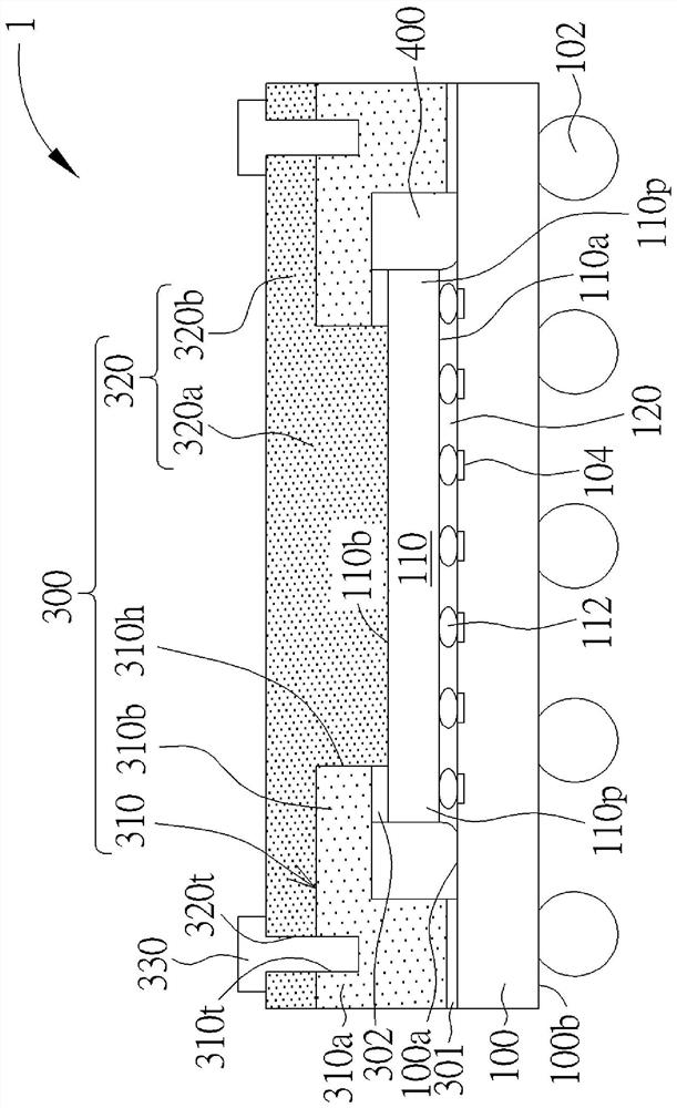
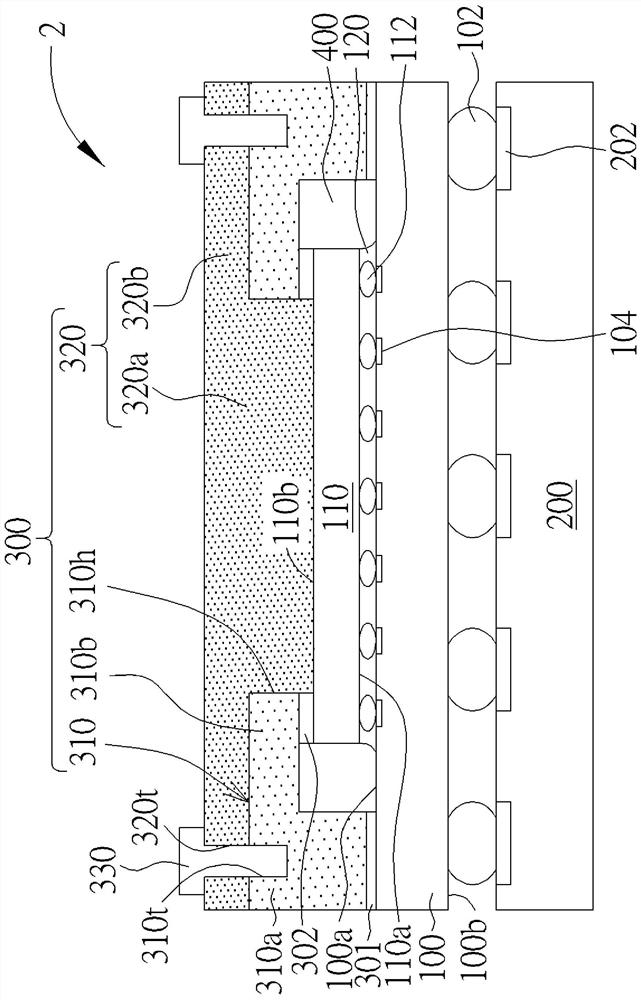
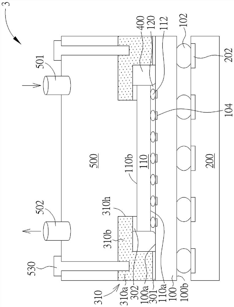
A semiconductor package includes a substrate having a top surface and a bottom surface; a semiconductor die mounted on the top surface of the substrate; and a cover mounted on a periphery of the top surface of the substrate and accommodating the semiconductor die, in which the cover includes an annular cover base and a cover plate detachably mounted on the annular cover base. By adopting the mode, after the semiconductor package is mounted on the printed circuit board, the detachably mounted cover plate can be removed, and other devices for cooling, such as a forced cooling module and the like, are mounted, so that the semiconductor package and semiconductor crystal grains in the semiconductor package are more efficiently cooled, the heat dissipation efficiency is improved, and the service life of the semiconductor package is prolonged. And the stability and high efficiency of working and running of the semiconductor crystal grains are ensured.

Description

technical field [0001] The invention relates to the technical field of semiconductors, in particular to a semiconductor package and a printed circuit board assembly. Background technique [0002] As the integration level of integrated circuit (integrated circuit, IC) devices driven by the demand for higher performance continues to increase, all application-level IC devices integrate more circuit elements per unit area. The need for smaller package sizes and higher device densities has also led to higher power densities, while the need for efficient heat dissipation has become paramount. [0003] Managing the heat generated by operating semiconductor chips has become an important technical issue. As temperatures rise, chip failure rates increase, and heat can cause permanent damage to semiconductor chips. Therefore, effective heat dissipation becomes a key issue in semiconductor packaging. [0004] As the power levels and heat generation of high-performance CPUs (central p...

Claims


Application Information

Patent Timeline
Patent Type & Authority Applications(China)
IPC IPC(8): H01L23/40H01L23/467H01L23/473H01L23/04H01L23/06H01L23/08H01L23/10H05K1/18
CPCH01L23/4006H01L23/4093H01L23/40H01L23/467H01L23/473H01L23/04H01L23/06H01L23/08H01L23/10H05K1/181H01L23/36H01L23/562H01L23/16H01L23/053H01L24/16H01L2224/16227H01L2224/32245H01L2224/29035H01L2224/32225H01L2224/73204H01L2224/2919H01L2224/33181H01L24/32H01L2224/73253H01L2924/00014H01L2224/16225H01L2924/00H01L23/31H05K5/0052H05K5/0221H05K5/03
Inventor 邱士超陈麒元许文松谢亚叡许耀邦黄文浚
Owner MEDIATEK INC
Learn More