Semiconductor module

A technology of semiconductors and molded parts, which is applied in the field of semiconductor modules and can solve problems that hinder the miniaturization of mounting substrates

Pending Publication Date: 2022-05-13
DENSO CORP
View PDF3 Cites 0 Cited by
  • Summary
  • Abstract
  • Description
  • Claims
  • Application Information

AI Technical Summary

Problems solved by technology

Securing this space hinders the miniaturization of the mounting substrate

Method used


Image

  • Semiconductor module
  • Semiconductor module
  • Semiconductor module

Examples


no. 1 approach

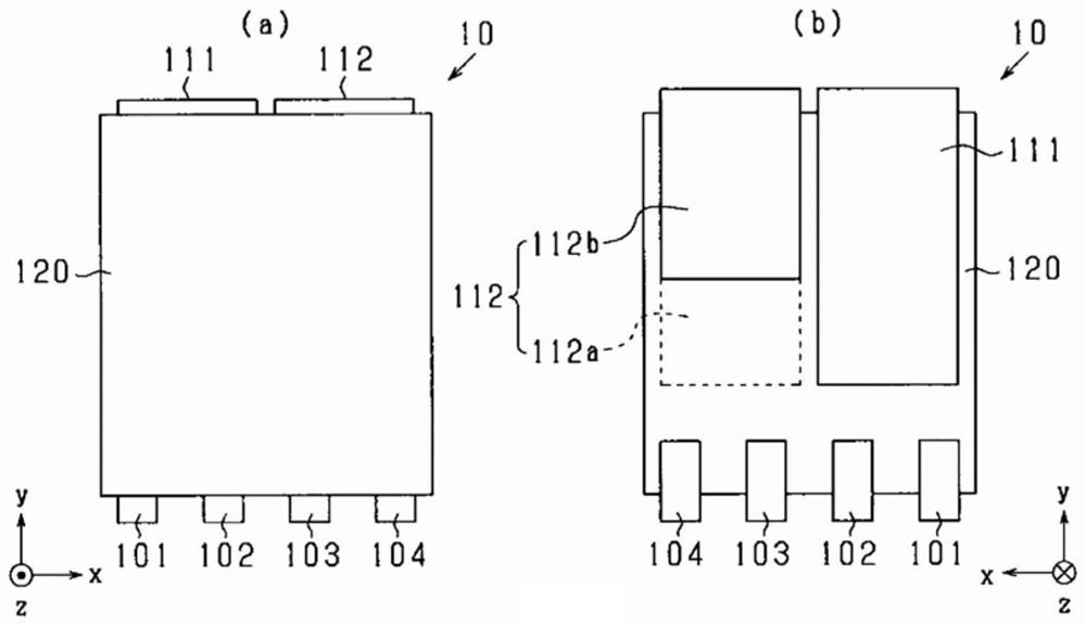
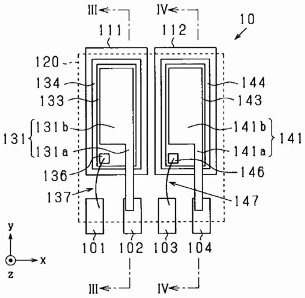
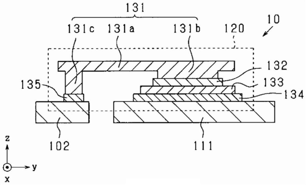
[0058] Such as Figure 1~5 As shown, the semiconductor module 10 according to the first embodiment includes a first semiconductor element 133 and a second semiconductor element 143, a resin mold 120 integrally sealing the first semiconductor element 133 and the second semiconductor element 143, and a conductive member 101. ~ 104, and conductive components 111, 112, 131, 141. Figure 1~5 The shown x-direction and y-direction are the lateral sides of the semiconductor module 10 , the xy plane direction is the planar direction of the semiconductor module 10 . The z direction is an up and down direction perpendicular to the planar direction.

[0059] Such as figure 1 As shown in (a), the semiconductor module 10 has four external terminals protruding in the negative direction of the y-axis and two external terminals protruding in the positive direction of the y-axis from the resin mold 120 having a substantially rectangular shape in plan view. Exterior. The four external termin...

no. 2 approach

[0096] In the first embodiment, a plurality of semiconductor elements (the first semiconductor element 133 and the second semiconductor element 143 ) were exemplified and arranged in the same orientation as the semiconductor elements adjacent to each other in a state substantially parallel to the adjacent semiconductor elements and Although described, like the second embodiment, they may be arranged in a direction opposite to that of the adjacent semiconductor elements so as to be approximately point-symmetrical to the adjacent semiconductor elements.

[0097]In the semiconductor module 20 according to the second embodiment, as Figures 12 to 15 As shown, in the resin mold 220, the second semiconductor element 243 and the first semiconductor element 233 are in an orientation in which the second semiconductor element 243 is rotated by 180° about the vertical direction (z direction) relative to the first semiconductor element 233. They are integrally sealed in a state aligned an...

no. 3 approach

[0112] In the first embodiment and the second embodiment, the conductive members are aligned and arranged in the direction (x direction) perpendicular to the direction (y direction) in which the external terminals protrude for the plurality of semiconductor elements, but they may also be arranged in the direction The directions in which the external terminals protrude are aligned and arranged.

[0113] In the semiconductor module 30 according to the third embodiment, as Figure 20-23 As shown, in the resin molded part 320, the second semiconductor element 343 and the first semiconductor element 333 are in an orientation in which the second semiconductor element 343 is rotated by 180° with respect to the first semiconductor element 333 in the vertical direction (z direction). They are integrally sealed in a state aligned and arranged in the y direction. That is, the first semiconductor element 333 and the second semiconductor element 343 are arranged in opposite directions to ...


PUM


Abstract

A semiconductor module (10) includes a plurality of semiconductor elements including a gate electrode, a first electrode, and a second electrode, a resin molded article (120), and a plurality of conductive members including: a common wiring electrode (111) exposed from the resin molded article on an upper surface side or a lower surface side of the semiconductor module; the second electrode is electrically connected to at least one of the first electrode and the second electrode. And non-common wiring electrodes (101-104) exposed from the resin mold and electrically connected to the electrodes of the semiconductor elements different from the common wiring electrodes, the wiring width of a common electrode connected to the common wiring electrodes being wider than the wiring width of the non-common wiring electrodes, and the plurality of semiconductor elements and the plurality of conductive members being disposed on the non-common wiring electrodes. When the common wiring is connected to the common wiring electrode, the common wiring can be provided from one side to the other side of the surface of the resin mold exposed from the common wiring electrode without being electrically connected to the non-common wiring electrode.

Description

[0001] Cross References to Related Applications [0002] This application is based on Japanese application No. 2019-181704 filed on October 1, 2019, and Japanese application No. 2020-160930 filed on September 25, 2020, the contents of which are cited here. technical field [0003] The invention relates to a semiconductor module comprising a plurality of semiconductor elements. Background technique [0004] Patent Document 1 describes a semiconductor module in which six semiconductor elements are included in one resin mold. In this semiconductor module, six semiconductor elements are power transistors and function as switching elements on the upper or lower arms of U, V, and W phases. [0005] Patent Document 1: Japanese Patent Laid-Open No. 2017-152727 [0006] In Patent Document 1, in order to connect three semiconductor elements, wiring is drawn out in a planar direction on lateral sides of the semiconductor elements, and semiconductor elements are connected to the drawn...

Claims


Application Information

Patent Timeline
IPC IPC(8): H01L25/07H01L25/18H01L23/29H01L23/31H01L29/78H02M7/00H02M7/48B62D5/04
CPCH01L25/072H01L25/18H01L23/3107H01L23/295H01L29/7813H02M7/003H02M7/48B62D5/04H01L2224/40245H01L2224/73265H01L2224/48247H01L2224/32245H01L2224/0603H01L29/12H01L29/78H01L23/49562H01L23/49524H01L23/49575B62D5/0406H01L23/3135H01L23/043H01L2224/73221H01L24/48H01L24/40H01L2924/00014H01L2224/45014H01L2924/181H01L2224/48091H01L24/37H01L2224/3701H01L24/32H01L24/73H02M7/5387H01L2224/45099H01L2924/00012H01L2924/00H01L23/49513H01L23/49568
Inventor 宫地修平藤田敏博斋藤敦长濑昇
Owner DENSO CORP
Why Eureka
Try Eureka