
Backlight module, preparation method thereof and display device

A technology for backlight modules and encapsulation adhesives, applied in optics, nonlinear optics, instruments, etc., can solve the problems of large gap between two substrates and optical crosstalk, and achieve the effect of reducing distance, eliminating gap and reducing optical crosstalk.

Pending Publication Date: 2022-05-17
广州华星光电半导体显示技术有限公司
View PDF13 Cites 0 Cited by
  • Summary
  • Abstract
  • Description
  • Claims
  • Application Information

AI Technical Summary

Problems solved by technology

[0004] Embodiments of the present application provide a backlight module, its manufacturing method, and a display device, so as to solve the problem that the existing gap between two substrates is usually large and optical crosstalk is likely to occur

Method used


Image

  • Backlight module, preparation method thereof and display device
  • Backlight module, preparation method thereof and display device
  • Backlight module, preparation method thereof and display device

Examples


Embodiment Construction

[0047] The technical solutions in the embodiments of the present application will be clearly and completely described below in conjunction with the drawings in the embodiments of the present application. Apparently, the described embodiments are only some of the embodiments of this application, not all of them. Based on the embodiments in this application, all other embodiments obtained by those skilled in the art without making creative efforts belong to the scope of protection of this application.

[0048] In order to solve the existing problem that the gap between two substrates is usually large and optical crosstalk is likely to occur, embodiments of the present application provide a backlight module, a manufacturing method thereof, and a display device, which will be described below with reference to the accompanying drawings.

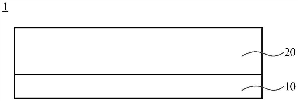
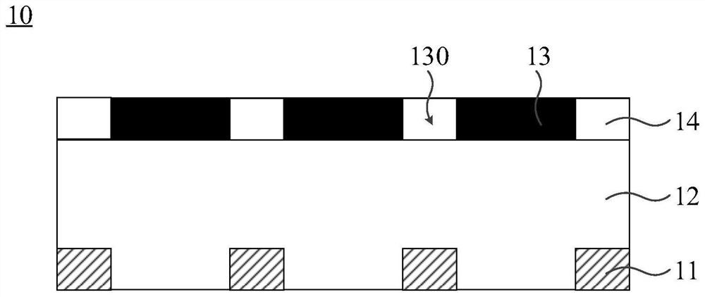
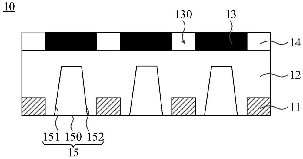
[0049] Exemplary, see figure 1 , figure 1 A schematic structural diagram of a display device provided in an embodiment of the present applicati...


PUM


Abstract

The embodiment of the invention provides a backlight module, a preparation method of the backlight module and a display device, and the backlight module comprises a plurality of mini-LED chips which are arranged at intervals; the packaging adhesive layer is arranged on all the mini-LED chips, and the space between every two adjacent mini-LED chips is filled with the packaging adhesive layer; the light absorption layer is arranged on the side, away from the mini-LED chips, of the packaging adhesive layer, a plurality of through holes are formed in the light absorption layer, and the through holes correspond to the mini-LED chips one to one; and the quantum dots are arranged in at least one through hole. The quantum dots are arranged on the side, deviating from the mini-LED chip, of the packaging adhesive layer, the scheme that the quantum dots are arranged on the color film substrate and then attached to the array substrate in a paired mode is replaced, the gap between the two substrates can be eliminated, the distance between the quantum dots and the mini-LED chip is reduced, and the yield of the LED is improved. And the problem of light crosstalk caused by a large gap between the two substrates between the adjacent mini-LED chips is further reduced.

Description

technical field [0001] The present application belongs to the field of display technology, and in particular relates to a backlight module, a manufacturing method thereof, and a display device. Background technique [0002] For a liquid crystal display device, a backlight module is usually required to provide a backlight source. Due to the outstanding advantages of mini-LED chips in display, performance, cost, etc., in some display devices, mini-LED chips are usually used as backlight sources. [0003] Wherein, in order to realize a wider color gamut display, QDs (Quantum Dots, quantum dots) are applied in a display device. In current display devices, quantum dots are usually arranged on a color filter substrate, and mini-LED chips are arranged on an array substrate. The color filter substrate and the array substrate need to be precisely aligned and bonded to realize a complete device. However, the gap between two substrates is usually large, which is prone to the problem ...

Claims


Application Information

Patent Timeline
IPC IPC(8): G02F1/13357G02F1/1333
CPCG02F1/133603G02F1/133606G02F1/133614G02F1/133605G02F1/1333
Inventor 崔霆飞
Owner 广州华星光电半导体显示技术有限公司
Learn More