Method for transferring disc type Micro-LED array on silicon substrate

A disk-shaped, silicon substrate technology, which is applied in the manufacture of semiconductor devices, electrical components, semiconductor/solid-state devices, etc., can solve the problems of LED chip damage, low transfer efficiency, complex process, etc., and achieve improved transfer efficiency and low material cost. The effect of low cost and simple transfer process

Pending Publication Date: 2022-05-17
BEIJING INST OF NANOENERGY & NANOSYST
View PDF4 Cites 0 Cited by
  • Summary
  • Abstract
  • Description
  • Claims
  • Application Information

AI Technical Summary

Problems solved by technology

[0011] The purpose of the present invention is to overcome the problems of high cost, complex process, low transfer efficiency and easy damage to LED chips in the process of substrate peeling, chip pick-up and precise transfer of existing Micro-LEDs. , providing a method for transferring a disk-shaped Micro-LED array on a silicon substrate, the method has the advantages of low material cost, stable and safe etching process, high processing precision, simple transfer process, high transfer efficiency and wide application

Method used


Image

  • Method for transferring disc type Micro-LED array on silicon substrate
  • Method for transferring disc type Micro-LED array on silicon substrate
  • Method for transferring disc type Micro-LED array on silicon substrate

Examples


Embodiment Construction

[0030] Neither the endpoints nor any values ​​of the ranges disclosed herein are limited to such precise ranges or values, and these ranges or values ​​are understood to include values ​​approaching these ranges or values. For numerical ranges, between the endpoints of each range, between the endpoints of each range and individual point values, and between individual point values ​​can be combined with each other to obtain one or more new numerical ranges, these values Ranges should be considered as specifically disclosed herein.

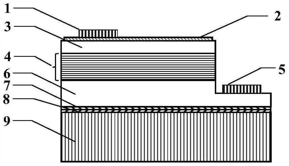
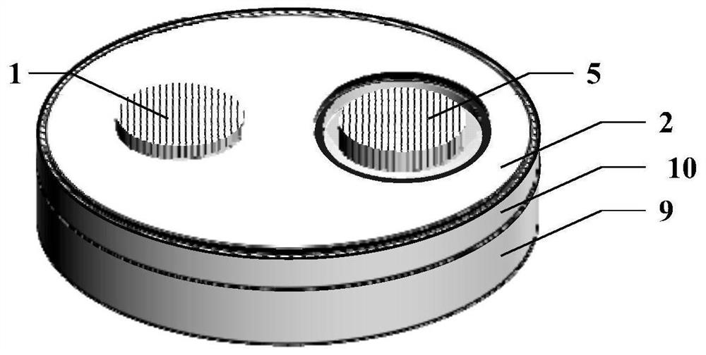
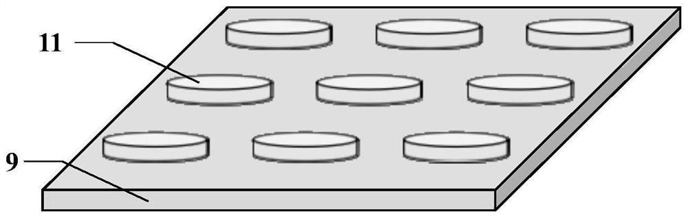
[0031] The present invention provides a method for transferring a disk-type Micro-LED array on a silicon substrate, which is characterized in that it includes the following steps:

[0032] (1) Protect the disk-shaped Micro-LED array on the silicon substrate by photolithography to obtain a Micro-LED array covered with photoresist;

[0033] (2) dry-etching the Micro-LED array covered with photoresist to obtain a suspended disk-type Micro-LED array su...


PUM

PropertyMeasurementUnit
diameteraaaaaaaaaa
thermal resistanceaaaaaaaaaa
thicknessaaaaaaaaaa

Abstract

The invention relates to the field of Micro-LED array transfer, and discloses a method for transferring a disc type Micro-LED array on a silicon substrate. The method comprises the following steps: (1) carrying out photoetching protection on a disc type Micro-LED array on a silicon substrate to obtain a Micro-LED array covered with photoresist; (2) the Micro-LED array covered with the photoresist is subjected to dry etching, and a suspended disc type Micro-LED array supported by a silicon column is obtained; and (3) photoresist removal, silicon substrate stripping and flexible transfer are carried out on the suspended disc-type Micro-LED array, and the suspended disc-type Micro-LED array is transferred to a target substrate. The method provided by the invention has the advantages of low material cost, stable and safe etching process, high processing precision, high transfer efficiency and wide application.

Description

technical field [0001] The invention relates to the field of Micro-LED array transfer, in particular to a method for transferring a disk-shaped Micro-LED array on a silicon substrate. Background technique [0002] At present, Micro-LED display is considered to be the next-generation display technology after LCD and OLED. It has the characteristics of self-illumination and does not require a backlight. Compared with OLED, the color is easier to adjust and has a higher resolution (1500ppi). , Faster response speed (ns level), longer life and higher brightness. [0003] Micro-LED is to prepare ultra-small LED chips and transfer a large number of LED chips to the driving substrate in an array, and control the brightness of each LED chip through the driving substrate. The preparation of Micro-LED mainly includes micro-process technology, mass transfer technology, bonding technology and color packaging. Among them, the mass transfer technology is the most difficult, and the LED c...

Claims


Application Information

Patent Timeline
Patent Type & Authority Applications(China)
IPC IPC(8): H01L33/00H01L33/48H01L21/67
CPCH01L33/0093H01L33/0095H01L21/67132H01L33/48H01L2933/0033H01L2224/95001
Inventor 王江文胡卫国化麒麟
Owner BEIJING INST OF NANOENERGY & NANOSYST
Why Eureka
Try Eureka