
PCB defect detection method and device, computer equipment and storage medium

A defect detection and detection method technology, applied in the field of image processing, can solve problems such as defect over-inspection, defect missed inspection, inability to guarantee inspection quality, etc., and achieve the effect of improving accuracy and automation.

Pending Publication Date: 2022-06-03
CHENGDU UNION BIG DATA TECH CO LTD
View PDF0 Cites 2 Cited by
  • Summary
  • Abstract
  • Description
  • Claims
  • Application Information

AI Technical Summary

Problems solved by technology

For the detection of defects in the PCB industry, the traditional solution adopts the method of visual inspection by personnel, which is very subjective, and it is easy to cause defects to be over-inspected or missed, and the quality of inspection cannot be guaranteed.

Method used


Image

  • PCB defect detection method and device, computer equipment and storage medium
  • PCB defect detection method and device, computer equipment and storage medium
  • PCB defect detection method and device, computer equipment and storage medium

Examples


Embodiment Construction

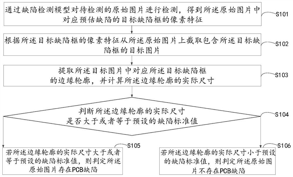
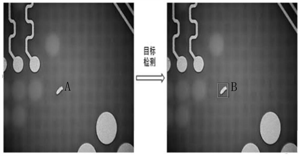
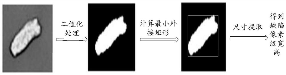
[0046] The technical solutions in the embodiments of the present invention will be clearly and completely described below with reference to the accompanying drawings in the embodiments of the present invention. Obviously, the described embodiments are only a part of the embodiments of the present invention, but not all of the embodiments.

[0047] The components of the embodiments of the invention generally described and illustrated in the drawings herein may be arranged and designed in a variety of different configurations. Thus, the following detailed description of the embodiments of the invention provided in the accompanying drawings is not intended to limit the scope of the invention as claimed, but is merely representative of selected embodiments of the invention. Based on the embodiments of the present invention, all other embodiments obtained by those skilled in the art without creative work fall within the protection scope of the present invention.

[0048] Hereinafte...


PUM


Abstract

The invention provides a PCB defect detection method and device, computer equipment and a storage medium, and relates to the technical field of image processing. According to the method, the original picture is detected through the defect detection model to obtain the pixel features of the target defect frame corresponding to the pre-estimated defect in the picture, the target picture containing the target defect frame is intercepted, the edge contour of the target defect frame is extracted, and the actual size of the edge contour is calculated; whether the actual size of the edge contour is larger than or equal to a preset defect standard value or not is judged, if the actual size is larger than or equal to the defect standard value, it is judged that the original picture has PCB defects, and if the actual size is smaller than the defect standard value, it is judged that the original picture does not have PCB defects. According to the invention, accurate positioning and quantitative evaluation of PCB defects can be realized, and the accuracy and automation degree of PCB detection are improved.

Description

technical field [0001] The present application relates to the technical field of image processing, and in particular to a PCB defect detection method, device, computer equipment and storage medium. Background technique [0002] The manufacturing process of Printed Circuit Board (PCB for short) consists of multiple stages, and various product defects, such as free copper defects, are easily introduced in the complex and cumbersome manufacturing process. These defects have different impacts on the product. When evaluating the defects, the manufacturer will also divide the defects into qualified and unqualified categories according to the defect type, defect size, defect proportion and other information, so as to ensure that the finished product is free of defects. Therefore, it is very necessary to accurately classify and quantitatively evaluate the defects on the printed circuit board. For the detection of defects in the PCB industry, the traditional solution adopts the meth...

Claims


Application Information

Patent Timeline
Patent Type & Authority Applications(China)
IPC IPC(8): G06T7/00G06T7/13G01N21/956
CPCG06T7/0006G06T7/13G01N21/956G01N21/95607G06T2207/20084G06T2207/20081G06T2207/30148G01N2021/95638G01N2021/95615Y02P90/30
Inventor 不公告发明人
Owner CHENGDU UNION BIG DATA TECH CO LTD
Features
  • Generate Ideas
  • Intellectual Property
  • Life Sciences
  • Materials
  • Tech Scout
  • Unparalleled Data Quality
  • Higher Quality Content
  • 60% Fewer Hallucinations
Learn More