Display panel and preparation method thereof
A display panel and panel technology, applied in semiconductor/solid-state device manufacturing, semiconductor devices, electrical components, etc.
- Summary
- Abstract
- Description
- Claims
- Application Information
AI Technical Summary
Problems solved by technology
Method used
Image

Examples
preparation example Construction
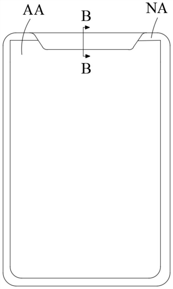
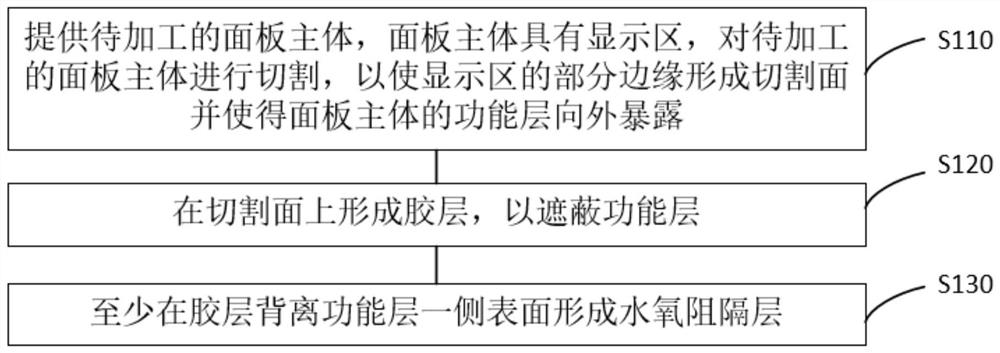
[0048] The present invention also provides a method for preparing a display panel. The display panel has a display area AA, which includes the following steps:
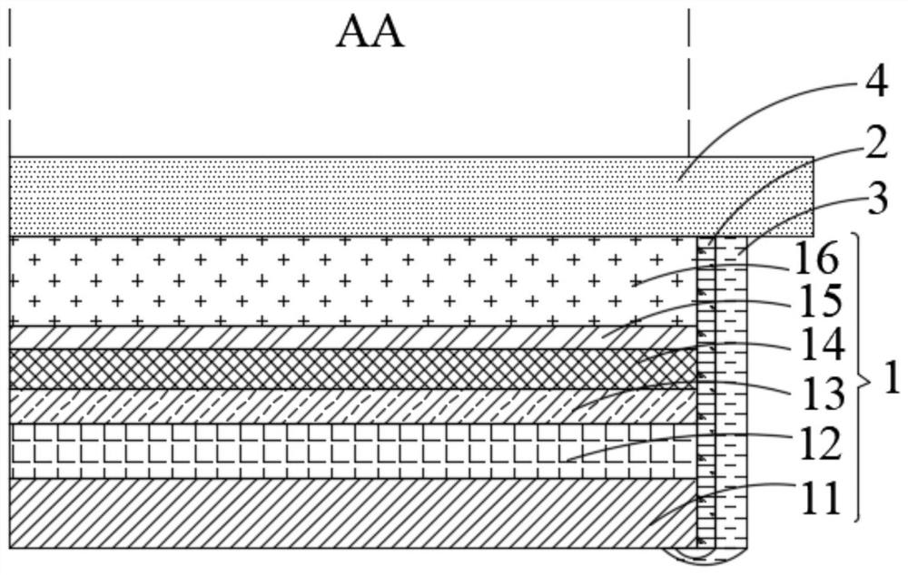
[0049] S110: Provide a panel body 1 to be processed, the panel body 1 has a display area AA, and cut the panel body 1 to be processed so that a part of the edge of the display area AA forms a cut surface and exposes the functional layer of the panel body 1 to the outside, like Figure 4 to Figure 7 shown, where, Figure 4 and Figure 5 It is a schematic structural diagram and a film layer structure diagram of the panel main body 1 before cutting, Image 6 and Figure 7 It is a schematic structural diagram and a film layer structure diagram of the panel main body 1 after cutting. By comparison, it can be seen that the encapsulation layer 14 of the panel main body 1 in the non-display area NA and the film layer in the display area AA are both cut and removed after cutting.
[0050] S120: Form an adhesive layer 2 on ...
PUM
 Abstract
Description
Claims
Application Information
 - R&D Engineer
- R&D Manager
- IP Professional
- Industry Leading Data Capabilities
- Powerful AI technology
- Patent DNA Extraction
Browse by: Latest US Patents, China's latest patents, Technical Efficacy Thesaurus, Application Domain, Technology Topic.
© 2024 PatSnap. All rights reserved.Legal|Privacy policy|Modern Slavery Act Transparency Statement|Sitemap