

Flexible device packaging structure and packaging method
A technology of flexible devices and packaging structures, which is applied in the direction of assembling printed circuits with electrical components, electrical components, and printed circuit components, etc. It can solve problems that affect the use of flexible devices, large packaging sizes, deformation of flexible devices, etc., and avoid connection failures , Guaranteed light loss, good sealing effect
- Summary
- Abstract
- Description
- Claims
- Application Information
AI Technical Summary
Problems solved by technology
Method used
Image

Examples
Embodiment Construction
[0034] The embodiments of the present invention will be described in detail below with reference to the accompanying drawings.
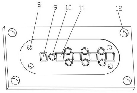
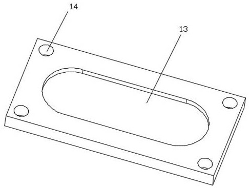
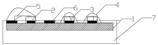
[0035] like Figure 1-5 As shown, a flexible device packaging structure includes a flexible circuit board 1 and a component 2 arranged on the flexible circuit board 1, and a gold wire 3 is formed between the component 2 and the flexible circuit board 1; A first encapsulation layer 5 is provided on the surface of the device 2, a second encapsulation layer 4 is arranged between the first encapsulation layer 5 and the flexible circuit board 1, and the flexible circuit board 1 is wrapped with a third encapsulation layer 7; the first encapsulation layer 5. The components 2 and the gold wires 3 are wrapped; the second encapsulation layer 4 is made of transparent material, and the second encapsulation layer 4 is formed on the surface of the first encapsulation layer 5; the third encapsulation layer 7 is a black structure, and the When the three encapsulati...
PUM
 Abstract
Description
Claims
Application Information