Supercharge Your Innovation With Domain-Expert AI Agents!

Bonding method of semiconductor

A bonding method and semiconductor technology, applied in semiconductor/solid-state device manufacturing, electrical components, circuits, etc., can solve problems such as product abnormality, damage, and impact on product quality, and achieve the effect of improving product quality and avoiding damage.

Pending Publication Date: 2022-07-01
SAE TECH DELEVOPMENT DONGGUAN
View PDF0 Cites 0 Cited by
  • Summary
  • Abstract
  • Description
  • Claims
  • Application Information

AI Technical Summary

Problems solved by technology

[0003] In the past welding process, the fixture is usually heated to melt the solder joints, and then the semiconductor is bonded. However, because the temperature of the fixture and the semiconductor drops too fast, the thermal expansion and contraction of the semiconductor in a short period of time often cause damage, resulting in The product is abnormal, which affects the product quality

Method used


Image

  • Bonding method of semiconductor

Examples


Embodiment Construction

[0015] The technical solutions in the embodiments of the present invention will be clearly and completely described below with reference to the accompanying drawings in the embodiments of the present invention. Obviously, the described embodiments are only a part of the embodiments of the present invention, but not all of the embodiments. Based on the embodiments of the present invention, all other embodiments obtained by persons of ordinary skill in the art without creative efforts shall fall within the protection scope of the present invention.

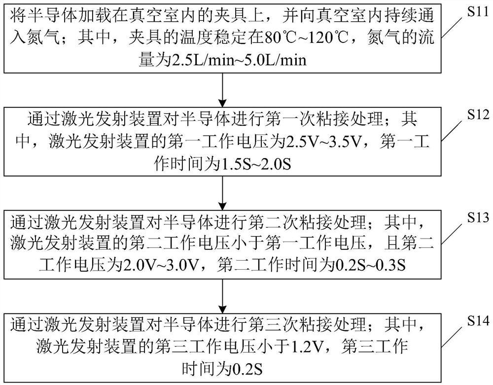
[0016] Embodiments of the present invention provide a method for bonding semiconductors, see figure 1 As shown, it is a flowchart of a preferred embodiment of a semiconductor bonding method provided by the present invention, and the method includes steps S11 to S14:

[0017] Step S11, loading the semiconductor on the fixture in the vacuum chamber, and continuously feeding nitrogen into the vacuum chamber; wherein, the temperature of...


PUM

PropertyMeasurementUnit
diameteraaaaaaaaaa

Abstract

The invention discloses a semiconductor bonding method which comprises the following steps: loading a semiconductor on a clamp in a vacuum chamber, and continuously introducing nitrogen into the vacuum chamber; wherein the temperature of the clamp is stabilized between 80 DEG C and 120 DEG C, and the flow rate of the nitrogen is 2.5 L / min to 5.0 L / min; carrying out first-time bonding treatment on the semiconductor through the laser emitting device; wherein the first working voltage of the laser emitting device ranges from 2.5 V to 3.5 V, and the first working time ranges from 1.5 S to 2.0 S; carrying out secondary bonding treatment on the semiconductor through the laser emitting device; wherein the second working voltage of the laser emitting device is smaller than the first working voltage, the second working voltage ranges from 2.0 V to 3.0 V, and the second working time ranges from 0.2 S to 0.3 S; carrying out third-time bonding treatment on the semiconductor through the laser emitting device; wherein the third working voltage of the laser emitting device is smaller than 1.2 V, and the third working time is 0.2 S. According to the technical scheme, the semiconductor can be gradually cooled during bonding, the semiconductor is prevented from being damaged, and therefore the product quality is improved.

Description

technical field [0001] The present invention relates to the technical field of semiconductor manufacturing, and in particular, to a method for bonding semiconductors. Background technique [0002] During the processing of semiconductor wafers, semiconductor products are usually bonded to a fixture for inspection. There are soldering points and lines on the fixture, and the contact points of the semiconductor are in contact with the soldering points on the fixture to complete various performance tests. [0003] In the past welding process, the fixture is usually heated, the solder joint is melted, and then the semiconductor is bonded. However, because the temperature of the fixture and the semiconductor drops too fast, the thermal expansion and cold contraction of the semiconductor in a short period of time often cause damage, resulting in The product is abnormal, which affects the quality of the product. SUMMARY OF THE INVENTION [0004] The technical problem to be solve...

Claims


Application Information

Patent Timeline
Patent Type & Authority Applications(China)
IPC IPC(8): H01L21/268H01L21/683
CPCH01L21/268H01L21/6835H01L2221/68304
Inventor 张俊群
Owner SAE TECH DELEVOPMENT DONGGUAN
Features
  • R&D
  • Intellectual Property
  • Life Sciences
  • Materials
  • Tech Scout
  • Unparalleled Data Quality
  • Higher Quality Content
  • 60% Fewer Hallucinations
Learn More