
Light-emitting substrate and manufacturing method thereof

A manufacturing method and substrate technology, which is applied in the direction of semiconductor devices, electrical components, circuits, etc., can solve the problems of easy peeling of the ink layer, and achieve the effects of improving insufficient curing, avoiding peeling, and improving reactivity

Pending Publication Date: 2022-07-01
TCL CHINA STAR OPTOELECTRONICS TECH CO LTD
View PDF0 Cites 0 Cited by
  • Summary
  • Abstract
  • Description
  • Claims
  • Application Information

AI Technical Summary

Problems solved by technology

[0005] The purpose of this application is to provide a light-emitting substrate and its manufacturing method to solve the problem that the ink layer on the light-emitting substrate is easy to peel off

Method used


Image

  • Light-emitting substrate and manufacturing method thereof
  • Light-emitting substrate and manufacturing method thereof
  • Light-emitting substrate and manufacturing method thereof

Examples


Embodiment Construction

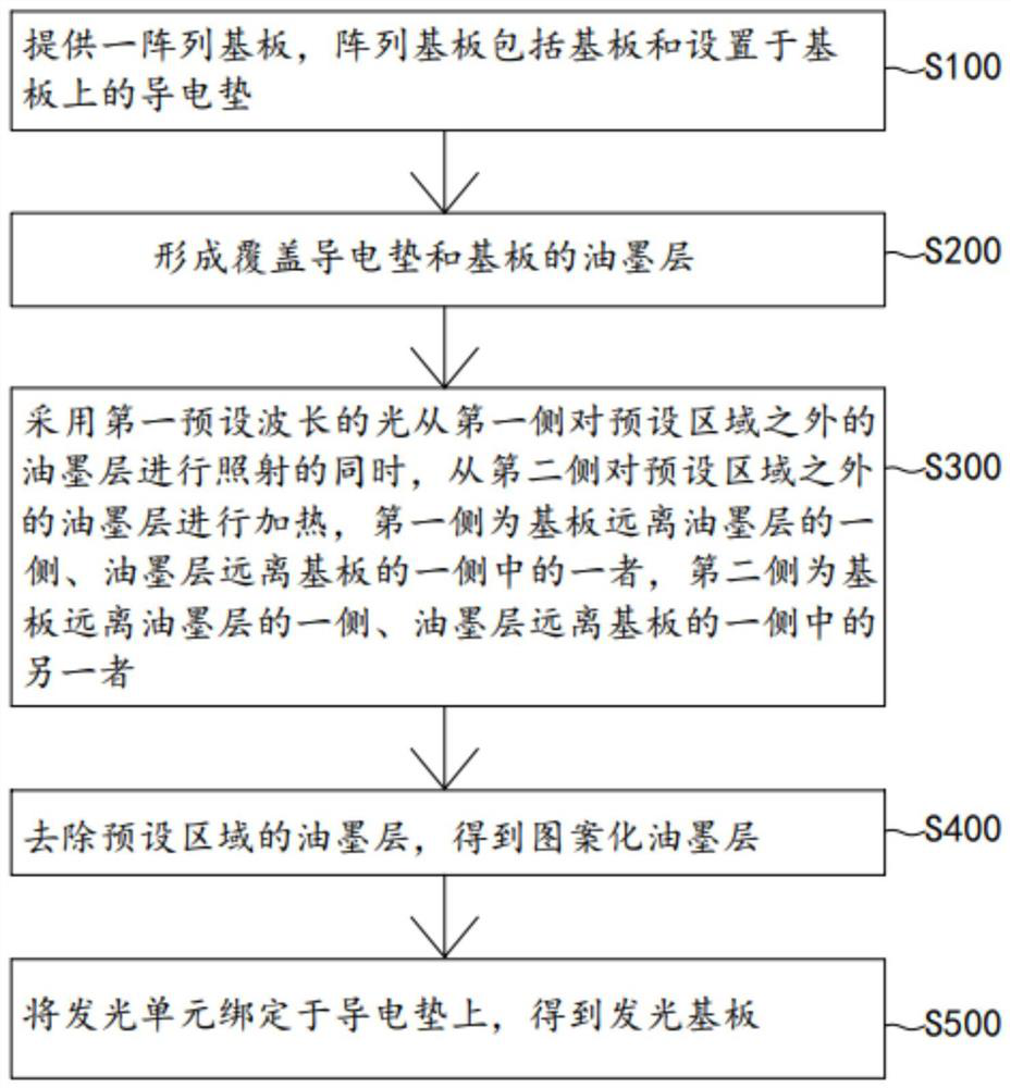
[0030] The technical solutions in the embodiments of the present application will be clearly and completely described below with reference to the accompanying drawings in the embodiments of the present application. Obviously, the described embodiments are only a part of the embodiments of the present application, but not all of the embodiments. Based on the embodiments in this application, all other embodiments obtained by those skilled in the art without creative efforts shall fall within the protection scope of this application.

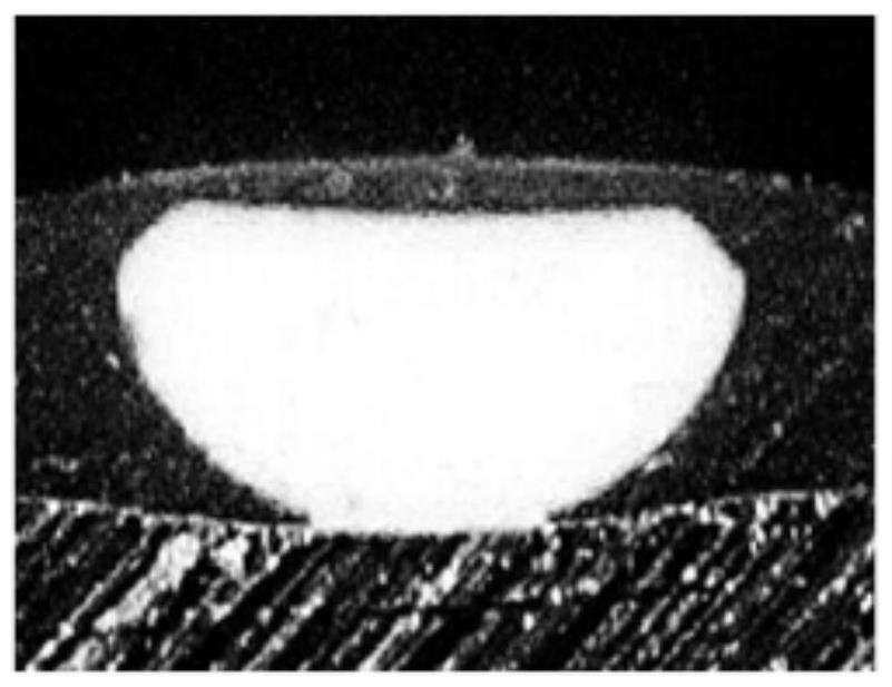
[0031] In view of the problem that the white ink layer is easily peeled off in the background technology, the inventors of the present application observed the peeled white ink layer, such as figure 1 As shown, the bottom of the peeled white ink layer includes an undercut structure ( figure 1 the white part in the undercut structure), the white ink layer in the undercut structure is hollowed out. For this phenomenon, the inventor found through an...


PUM

PropertyMeasurementUnit
Wavelengthaaaaaaaaaa
Thicknessaaaaaaaaaa

Abstract

The invention discloses a light-emitting substrate and a manufacturing method thereof, and the method comprises the steps: providing an array substrate which comprises a substrate and a conductive pad disposed on the substrate; an ink layer covering the conductive pad and the substrate is formed, the ink layer comprises a preset area, and the preset area corresponds to the conductive pad in position; the ink layer outside the preset area is heated from a second side while light with a first preset wavelength is adopted to irradiate the ink layer outside the preset area from a first side, the first side is one of the side, away from the ink layer, of the substrate and the side, away from the substrate, of the ink layer, and the second side is one of the side, away from the substrate, of the ink layer; the second side is the other one of the side, away from the ink layer, of the substrate and the side, away from the substrate, of the ink layer; removing the ink layer in the preset area to obtain a patterned ink layer; and binding the light-emitting unit on the conductive pad to obtain the light-emitting substrate.

Description

technical field [0001] The present application relates to the field of display technology, and in particular, to a light-emitting substrate and a manufacturing method thereof. Background technique [0002] Active sub-millimeter light-emitting diode displays have the characteristics of high brightness, strong grayscale performance, high color saturation, and high-definition dynamic picture quality, plus their unique advantages of easy storage and installation, they can replace traditional monitors and projectors. [0003] Active sub-millimeter LED displays include a layer of white ink on the surface to prevent scratches. However, white ink has the problem of easy peeling, and white ink peeling can lead to the risk of interfacial corrosion on active sub-millimeter LED displays. . [0004] Therefore, it is necessary to propose a technical solution to solve the problem that a layer of white ink on the surface of the active sub-millimeter light emitting diode display is easily p...

Claims


Application Information

Patent Timeline
IPC IPC(8): H01L33/44H01L33/48H01L33/00
CPCH01L33/44H01L33/0095H01L33/48H01L2933/0025H01L2933/0033H01L25/167H01L27/1292
Inventor 赵永超
Owner TCL CHINA STAR OPTOELECTRONICS TECH CO LTD
Learn More