Semiconductor packaging element testing device

A technology for packaging components and testing devices, applied in the field of testing devices for semiconductor packaging components, can solve the problems of inconvenience in testing semiconductor packaging components, the test process is not smooth, and the semiconductor packaging components cannot be fixed, and the effects of preventing loosening and incomplete testing can be achieved.

Pending Publication Date: 2022-07-05
深圳市安润佳半导体科技有限公司
View PDF0 Cites 1 Cited by
  • Summary
  • Abstract
  • Description
  • Claims
  • Application Information

AI Technical Summary

Problems solved by technology

[0003] Common semiconductor packaging component testing devices, in the prior art, testers use spring probes, such as POGO needles, etc., to manually test semiconductor packaging components, because the semiconductor packaging components cannot be well tested during the test process. The fixation of the test process is

Method used


Image

  • Semiconductor packaging element testing device
  • Semiconductor packaging element testing device
  • Semiconductor packaging element testing device

Examples


Embodiment 1

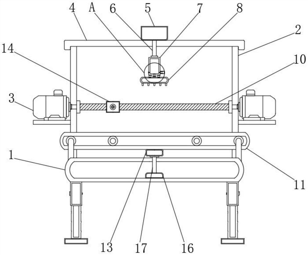
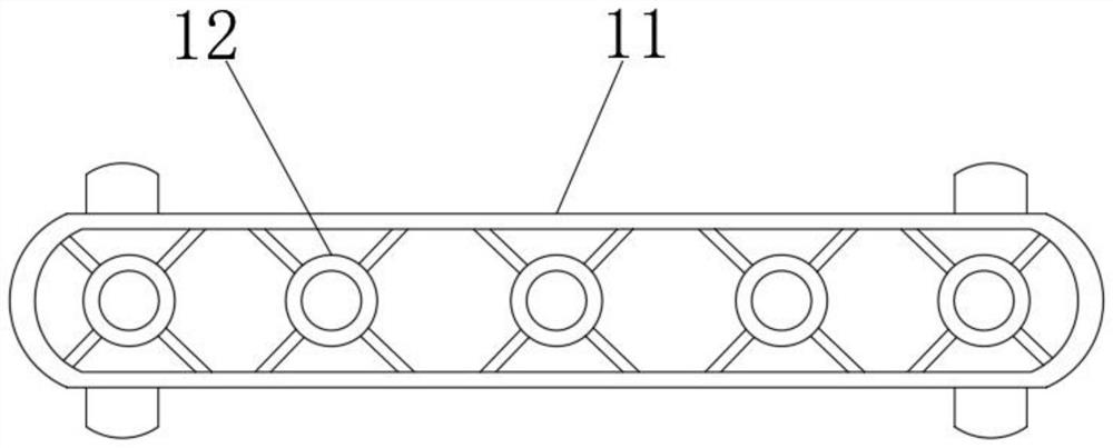
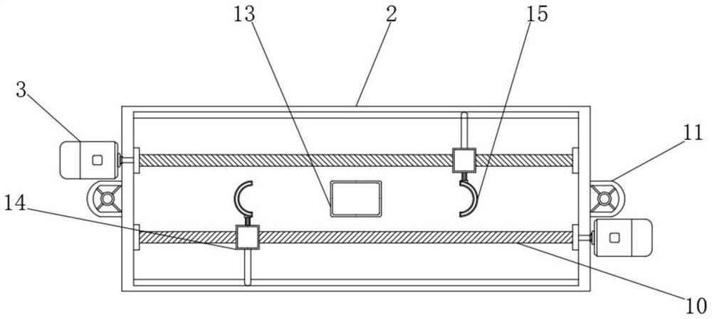
[0040] The present invention provides a technical solution, a semiconductor package component testing device, comprising a support base 1 , a fixed connection plate 2 , a drive motor 3 , a connection cover plate 4 , a first hydraulic cylinder 5 , a first piston rod 501 , and a connection column 7 , test board 8, test probe 9, threaded rod 10, conveyor belt 11, placement groove 12, test table 13, sliding connection block 14, semicircular clamp 15, second hydraulic cylinder 16, second piston rod 17, rotating gear 18 and translation tooth plate 19, see figure 1 , the top of the support base 1 is fixedly installed with a fixed connection plate 2, both sides of the fixed connection plate 2 are fixed with a drive motor 3, and the top of the fixed connection plate 2 is movably equipped with a connection cover plate 4, and the connection cover plate A first hydraulic cylinder 5 is movably installed at the top center position of the connecting cover plate 4, and a first piston rod 501 ...

Embodiment 2

[0044] On the basis of Example 1, as Figure 6-8 As shown, the lifting support column includes:

[0045] The fixed seat 6, the inner left and right sides of the fixed seat 6 are symmetrically provided with a movable cavity 1 601, a movable cavity 2 602, and a movable cavity 3 617, and the movable cavity 2 602 penetrates the upper end of the fixed seat 6 and communicates with the outside world, so The second movable cavity 602 is communicated with the third movable cavity 617, the left and right ends of the fixed seat 6 are symmetrically provided with open grooves 604, and the lower end of the open groove 604 is provided with a second groove;

[0046] Two rotating blocks 603, the two rotating blocks 603 are respectively rotated and arranged in the opening grooves 604 at the left and right ends, the lower end of the rotating block 603 is provided with a groove one 605, the groove one 605 and the groove The two are arranged correspondingly, and the second groove is slidably conn...

Embodiment 3

[0057] On the basis of embodiment 1, also include:

[0058] Force sensor 1: The force sensor 1 is arranged at one end of the semicircular fixture 15 on the left side away from the sliding connection block 14, and is used to detect the force that the semicircular fixture 15 on the left side receives during semiconductor testing;

[0059] Force sensor 2: The force sensor 2 is arranged at the end of the right semi-circular fixture 15 away from the sliding connection block 14, and is used to detect the force received by the right semi-circular fixture 15 during semiconductor testing;

[0060] Alarm: the alarm is arranged outside the support base 1;

[0061] Controller: the controller is electrically connected with the first force sensor, the second force sensor and the alarm;

[0062] The controller controls the alarm to work based on the first force sensor and the second force sensor, including the following steps:

[0063] Step 1: The controller calculates the theoretical allo...


PUM


Abstract

The invention relates to the technical field of packaging component testing, and discloses a semiconductor packaging component testing device.Fixed connecting plates are fixedly installed on the periphery of the top of a supporting base, driving motors are fixedly arranged on the two sides of each fixed connecting plate, and a connecting cover plate is movably arranged on the top of each fixed connecting plate; a first hydraulic cylinder is movably installed in the center of the top of the connecting cover plate, and a first piston rod is additionally and movably arranged in the center of the bottom of the connecting cover plate. According to the semiconductor packaging element testing device, after the additionally arranged first hydraulic cylinder is started, the testing probe tests the part of a semiconductor and ascends to a certain height, the servo motor is started to drive the rotating gear to rotate through the rotating rod, and when the rotating gear rotates, the testing plate is driven to translate through the meshed translation toothed plate. Multiple parts of a semiconductor can be conveniently tested, and the phenomenon that the product quality is reduced due to incomplete testing is prevented.

Description

technical field [0001] The invention relates to the technical field of package component testing, in particular to a semiconductor package component testing device. Background technique [0002] Semiconductor packaging refers to the process of processing the tested wafers according to the product model and functional requirements to obtain independent semiconductor packaging. The package form refers to a housing for mounting a semiconductor integrated circuit semiconductor. It not only plays the role of mounting, fixing, sealing, protecting the semiconductor and enhancing the electrical and thermal performance, but also connected to the pins of the package shell with wires through the contacts on the semiconductor, and these pins pass through the wires on the printed circuit board. It is connected with other devices to realize the connection between the internal semiconductor and the external circuit. After the second package is completed, the components need to be tested f...

Claims


Application Information

Patent Timeline
IPC IPC(8): G01R31/26G01R1/04
CPCG01R31/2601G01R1/0425
Inventor 赵晓美
Owner 深圳市安润佳半导体科技有限公司
Why Eureka
Try Eureka