
Display panel, manufacturing method thereof and display device

A technology for a display panel and a manufacturing method, which is applied in the manufacture of semiconductor/solid-state devices, semiconductor/solid-state device parts, semiconductor devices, etc., can solve the problems of blackening of alignment marks and difficulty in being recognized, and achieves the guarantee of flatness and reduced Effects of darkening and hard-to-recognize risks

Pending Publication Date: 2022-07-05
BOE TECH GRP CO LTD +1
View PDF0 Cites 0 Cited by
  • Summary
  • Abstract
  • Description
  • Claims
  • Application Information

AI Technical Summary

Problems solved by technology

[0004] In view of the shortcomings of the existing methods, the present application proposes a display panel, its manufacturing method, and a display device to solve the problem that the alignment marks in the display panel in the related art are blackened and difficult to be recognized

Method used


Image

  • Display panel, manufacturing method thereof and display device
  • Display panel, manufacturing method thereof and display device
  • Display panel, manufacturing method thereof and display device

Examples


Embodiment Construction

[0054] The application is described in detail below, and examples of embodiments of the application are illustrated in the accompanying drawings, wherein the same or similar reference numerals refer to the same or similar components or components having the same or similar functions throughout. Also, detailed descriptions of known technologies are omitted if they are not necessary for illustrating features of the present application. The embodiments described below with reference to the accompanying drawings are exemplary and are only used to explain the present application, but not to be construed as a limitation on the present application.

[0055]It will be understood by those skilled in the art that the singular forms "a", "an", "the" and "the" as used herein can include the plural forms as well, unless expressly stated otherwise. It should be further understood that the word "comprising" used in the specification of this application refers to the presence of stated featur...


PUM


Abstract

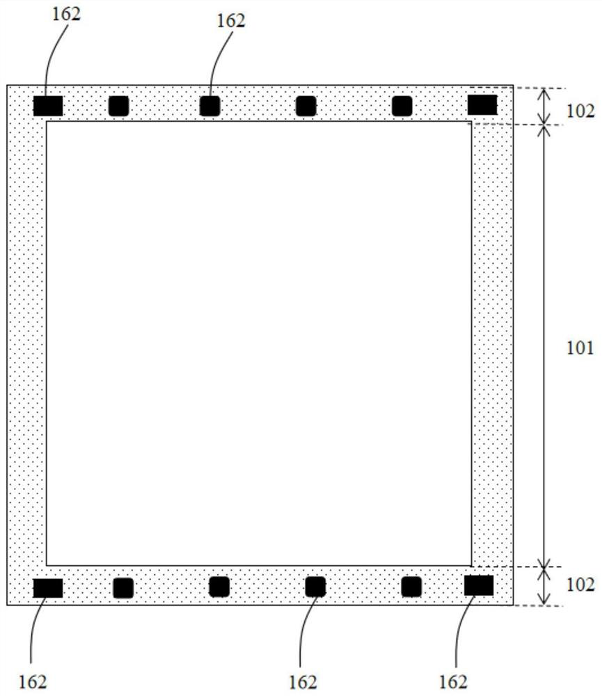
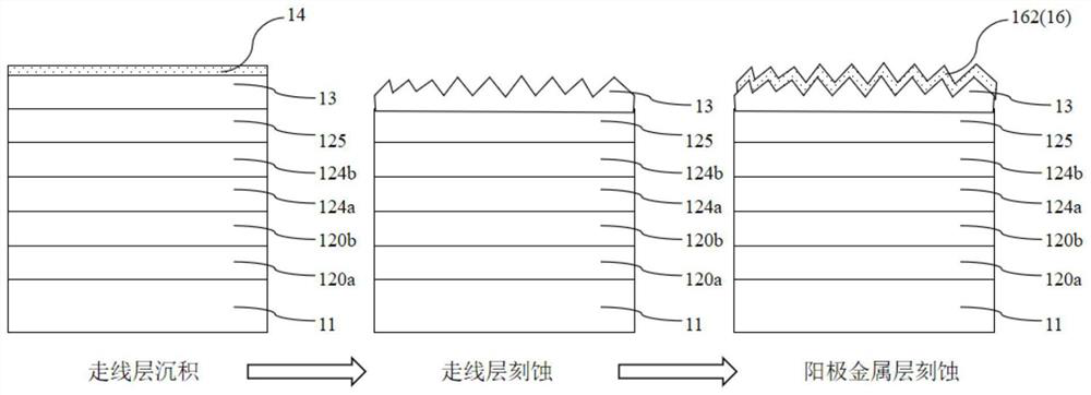
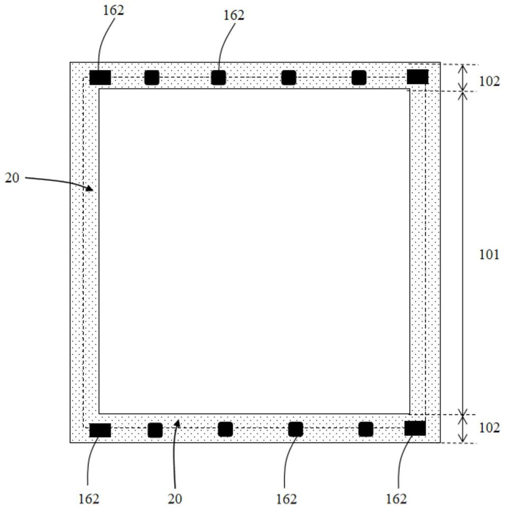
The embodiment of the invention provides a display panel, a manufacturing method thereof and a display device, the display panel comprises a display area and a peripheral area surrounding the display area, and the display panel comprises a substrate, a thin film transistor layer, a first planarization layer, a wiring layer, a second planarization layer and an anode metal layer which are stacked in sequence; the wiring layer is located in the display area, the first planarization layer and the second planarization layer extend from the display area to the peripheral area, and the anode metal layer comprises an anode layer located in the display area and an alignment mark located in the peripheral area. The two planarization layers are arranged in the display panel, the alignment mark is manufactured on the surface of the second planarization layer, the situation that when the alignment mark is manufactured on the first planarization layer, the alignment mark is not flat due to surface damage of the first planarization layer is avoided, the flatness of the alignment mark is guaranteed, and the display quality is improved. And the risk that the alignment mark becomes black and is difficult to identify is reduced.

Description

technical field [0001] The present application relates to the field of display technology, and in particular, the present application relates to a display panel, a manufacturing method thereof, and a display device. Background technique [0002] Optical functional film (such as OCA optical glue, polarizer, etc.) is one of the important components of the display panel. Its filming efficiency and film orientation accuracy affect the performance of the display panel, as well as the production cost. [0003] In the production process of the display panel, when the optical functional film is attached to the display panel, it is necessary to perform the alignment through the alignment marks provided on the display panel. However, the display panel in the related art is prone to the problem that the alignment mark is black and difficult to identify, resulting in inaccurate alignment when the optical functional film is attached, which affects the performance of the display panel. ...

Claims


Application Information

Patent Timeline
Patent Type & Authority Applications(China)
IPC IPC(8): H01L27/32H01L23/544H01L21/77
CPCH01L23/544H01L2223/54426H10K59/124H10K59/131H10K59/1201
Inventor 鲁栋良宋亮王江林胡静李信许家豪杨增刚韩文强姜龙张继川刘肖楠廖鹏宇李相喆赵吾阳史伟杰张宇
Owner BOE TECH GRP CO LTD
Learn More