Bonding method and bonding structure of semiconductor material

A bonding structure and semiconductor technology, applied in the direction of semiconductor devices, semiconductor/solid-state device manufacturing, electrical components, etc., can solve problems such as product failure, affecting device performance, and high heat treatment temperature requirements, so as to improve product reliability and ensure device performance, the effect of reducing bonding defects

Pending Publication Date: 2022-07-08
GALAXYCORE SHANGHAI
View PDF0 Cites 0 Cited by
  • Summary
  • Abstract
  • Description
  • Claims
  • Application Information

AI Technical Summary

Problems solved by technology

[0007] in, figure 1 The disadvantage of the bonding method shown is that the bonding strength is weak, and the post-bonding heat treatment temperature is higher (>950°C), which affects the device performance, and is prone to bonding defects such as bubbles and voids.
figure 2 , image 3 The bonding method shown can achieve strong bonding strength (>2J / m 2 ), and due to the absorption of gas by insulating media such as silicides, bonding defects such as bubbles and voids are reduced, but due to the isolation of insulating media at the bonding interface, the charges generated in the subsequent process cannot be transferred and eliminated, and will accumulate in the The surface of the substrate may cause arc effects, or some defects may cause product failure, machine pollution and other problems

Method used


Image

  • Bonding method and bonding structure of semiconductor material
  • Bonding method and bonding structure of semiconductor material
  • Bonding method and bonding structure of semiconductor material

Examples


Embodiment Construction

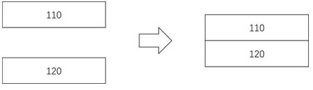
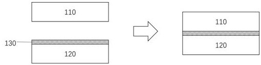
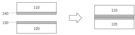
[0041] In order to solve the above-mentioned problems in the prior art, the present invention provides a bonding method and a bonding structure for semiconductor materials. By forming a mixed surface of a semiconductor medium and an insulating medium on at least one piece of semiconductor material, the bonding interface includes both semiconductor materials. The contact area between the medium and the semiconductor medium also includes the contact area between the semiconductor medium and the insulating medium and / or the contact area between the insulating medium and the insulating medium. The contact area between the semiconductor medium and the semiconductor medium is used for charge transfer to avoid problems such as arcing effect, product failure, and machine pollution caused by charge accumulation; the contact area between the semiconductor medium and the insulating medium and / or the contact area between the insulating medium and the insulating medium is used for It can ac...


PUM

PropertyMeasurementUnit
thicknessaaaaaaaaaa

Abstract

The invention provides a bonding method and a bonding structure of a semiconductor material, and the method comprises the steps: forming a mixed surface of a semiconductor medium and an insulating medium on at least one piece of semiconductor material, enabling a bonding interface to comprise a contact region of the semiconductor medium and a contact region of the insulating medium; and the contact area of the semiconductor medium and the insulating medium and/or the contact area of the insulating medium and the insulating medium are/is included. The contact area between the semiconductor media is used for charge transfer, so that the problems of arc effect, product failure, machine pollution and the like caused by charge accumulation are avoided; the contact area of the semiconductor medium and the insulating medium and/or the contact area of the insulating medium and the insulating medium are/is used for achieving high bonding strength at low temperature, bonding defects are reduced, device performance is guaranteed, and product reliability is improved.

Description

technical field [0001] The present invention relates to a bonding method and bonding structure of semiconductor materials. Background technique [0002] In order to meet the needs of further miniaturization and multi-functionalization of electronic products, integrated circuit manufacturing technology has developed rapidly, and the bonding process between semiconductor materials is increasingly used in the manufacturing process. [0003] Figure 1-Figure 3 Three main types of bonding between existing semiconductor materials (using silicon wafers as an example) are shown. [0004] like figure 1 As shown, after the first wafer 110 and the second wafer 120 are respectively planarized, they are directly bonded to each other to form a silicon-to-silicon bonding interface; [0005] like figure 2 As shown, an insulating dielectric film 130 such as silicon oxide, silicon nitride or silicon carbonitride is first deposited on the surface of the second wafer 120, and then bonded w...

Claims


Application Information

Patent Timeline
Patent Type & Authority Applications(China)
IPC IPC(8): H01L21/18H01L29/16
CPCH01L21/187H01L29/16
Inventor 赵立新李朝勇胡杏邹文邱裕明
Owner GALAXYCORE SHANGHAI
Why Eureka
Try Eureka