
Lead frame and manufacturing method thereof applied to semiconductor packaging structure

A technology of lead frames and semiconductors, applied in the field of lead frames, can solve problems such as electrical short circuits, achieve the effects of avoiding short circuits, increasing contact area, and reducing metal burrs

Pending Publication Date: 2022-07-08
CHIPMOS TECH INC
View PDF0 Cites 0 Cited by
  • Summary
  • Abstract
  • Description
  • Claims
  • Application Information

AI Technical Summary

Problems solved by technology

If there are many metal parts to be cut by the tool, based on the material characteristics of the metal lead frame, the cutting edge of the lead frame will easily be driven by the rotation of the tool to form metal burrs on the edge. In this way, there will be electrical potential risk of short circuit

Method used


Image

  • Lead frame and manufacturing method thereof applied to semiconductor packaging structure
  • Lead frame and manufacturing method thereof applied to semiconductor packaging structure
  • Lead frame and manufacturing method thereof applied to semiconductor packaging structure

Examples


Embodiment Construction

[0047] Reference will now be made in detail to the exemplary embodiments of the present invention, examples of which are illustrated in the accompanying drawings. Wherever possible, the same reference numerals are used in the drawings and description to refer to the same or like parts.

[0048] Exemplary embodiments of the present invention will be fully described below with reference to the accompanying drawings, but the present invention may also be embodied in many different forms and should not be construed as limited to the embodiments described herein. In the drawings, for the sake of clarity, the size and thickness of various regions, parts and layers may not be drawn to scale. In order to facilitate understanding, the same elements in the following description will be described with the same symbols.

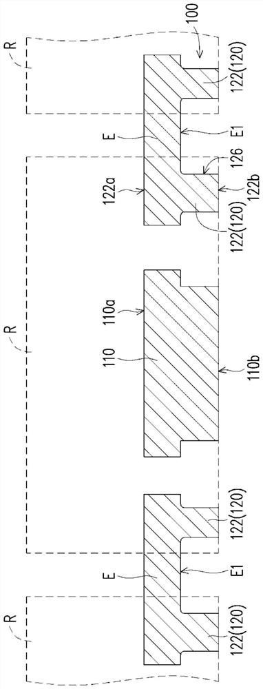
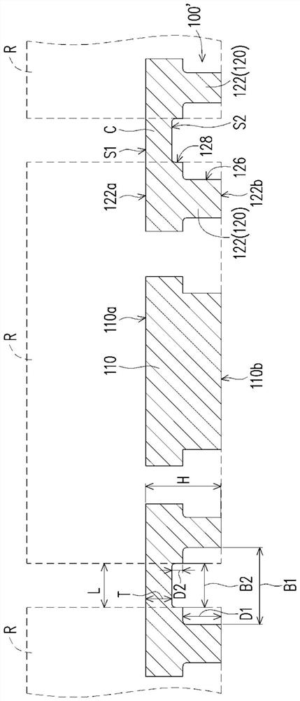
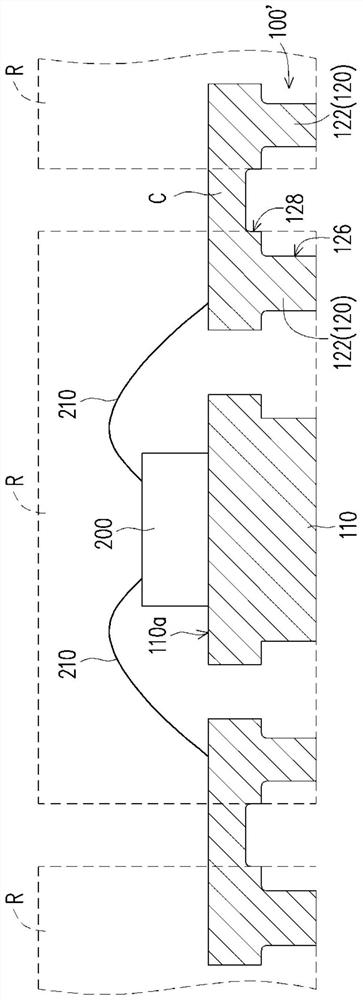
[0049] 1A to 1E It is a schematic cross-sectional view of a manufacturing method of a lead frame applied to a semiconductor package structure according to an embodimen...


PUM


Abstract

The invention provides a lead frame and a manufacturing method for applying the lead frame to a semiconductor packaging structure. The lead frame comprises a plurality of packaging areas and a plurality of connecting parts connected with the packaging areas. Each packaging area comprises a bearing seat and an outer pin part. The outer pin part surrounds the bearing seat and comprises a plurality of pins extending towards the periphery. Each connecting part is connected with the pins of the two adjacent outer pin parts, and a first groove and a second groove are defined by the connecting part and the two adjacent pins. The second grooves are located between the first grooves and the corresponding connecting parts, and the width of the second grooves is smaller than that of the first grooves. According to the lead frame and the manufacturing method for applying the lead frame to the semiconductor packaging structure, the generation of burrs can be reduced, and the combination of the packaging structure and the outside can be improved, so that the subsequent quality inspection is facilitated.

Description

technical field [0001] The invention relates to a lead frame, in particular to a lead frame and a manufacturing method thereof applied to a semiconductor packaging structure. Background technique [0002] In the current Small outline no-lead (SON) package, since the side of this package type is filled with encapsulation material, it only contacts with the external circuit board through the exposed local pins at the bottom of the package structure. way of electrical connection. Therefore, after being bonded to the external circuit board, since the electrically connected pins are located at the bottom of the package structure, the connection status with the circuit board cannot be confirmed through visual inspection, which is not conducive to subsequent electrical and quality inspections. In addition, during the cutting process of the package structure of the leadless small size package, the tool needs to cut off the side-by-side lead frames to form a single package structure...

Claims


Application Information

Patent Timeline
Patent Type & Authority Applications(China)
IPC IPC(8): H01L23/495H01L21/48
CPCH01L23/495H01L23/4952H01L21/4828H01L2224/48247H01L2924/181H01L2224/97H01L2924/00012
Inventor 古恒安吴佳蓉
Owner CHIPMOS TECH INC
Learn More