
Semiconductor wafer storage container

A technology for storage containers and semiconductors, applied in semiconductor/solid-state device manufacturing, packaging objects under special gas conditions, packaging object types, etc., can solve problems such as poor sealing effect, insufficient sealing method, and uneven force of the main body , to achieve the effect of facilitating extrusion and discharge and ensuring the sealing effect

Pending Publication Date: 2022-07-12
荣耀半导体材料(嘉善)有限公司
View PDF6 Cites 1 Cited by
  • Summary
  • Abstract
  • Description
  • Claims
  • Application Information

AI Technical Summary

Problems solved by technology

[0004] In the prior art, when the locking mechanism is rotated and locked, it can only be advanced in a straight line, so that it can only lock and seal one opposite side of the cover. The problem of uneven force, at the same time, when the lock seal is performed, the entire seal cannot maintain a good sealing effect
[0005] In addition, the sealing in the prior art is specifically to contact the polycarbonate material through the elastic seal, which is not sufficient and the sealing effect is not good

Method used


Image

  • Semiconductor wafer storage container
  • Semiconductor wafer storage container
  • Semiconductor wafer storage container

Examples


Embodiment Construction

[0045] In order to make the purposes, technical solutions and advantages of the embodiments of the present application more clear, the technical solutions in the embodiments of the present application will be described clearly and completely below with reference to the accompanying drawings in the embodiments of the present application. Obviously, the described embodiments are some, but not all, embodiments of the present application. The components of the embodiments of the present application generally described and illustrated in the drawings herein may be arranged and designed in a variety of different configurations.

[0046] In the description of this application, it should be noted that the orientation or positional relationship indicated by the terms "inside", "outside", etc. is based on the orientation or positional relationship shown in the accompanying drawings, or is usually placed when the product of the application is used. The orientation or positional relations...


PUM


Abstract

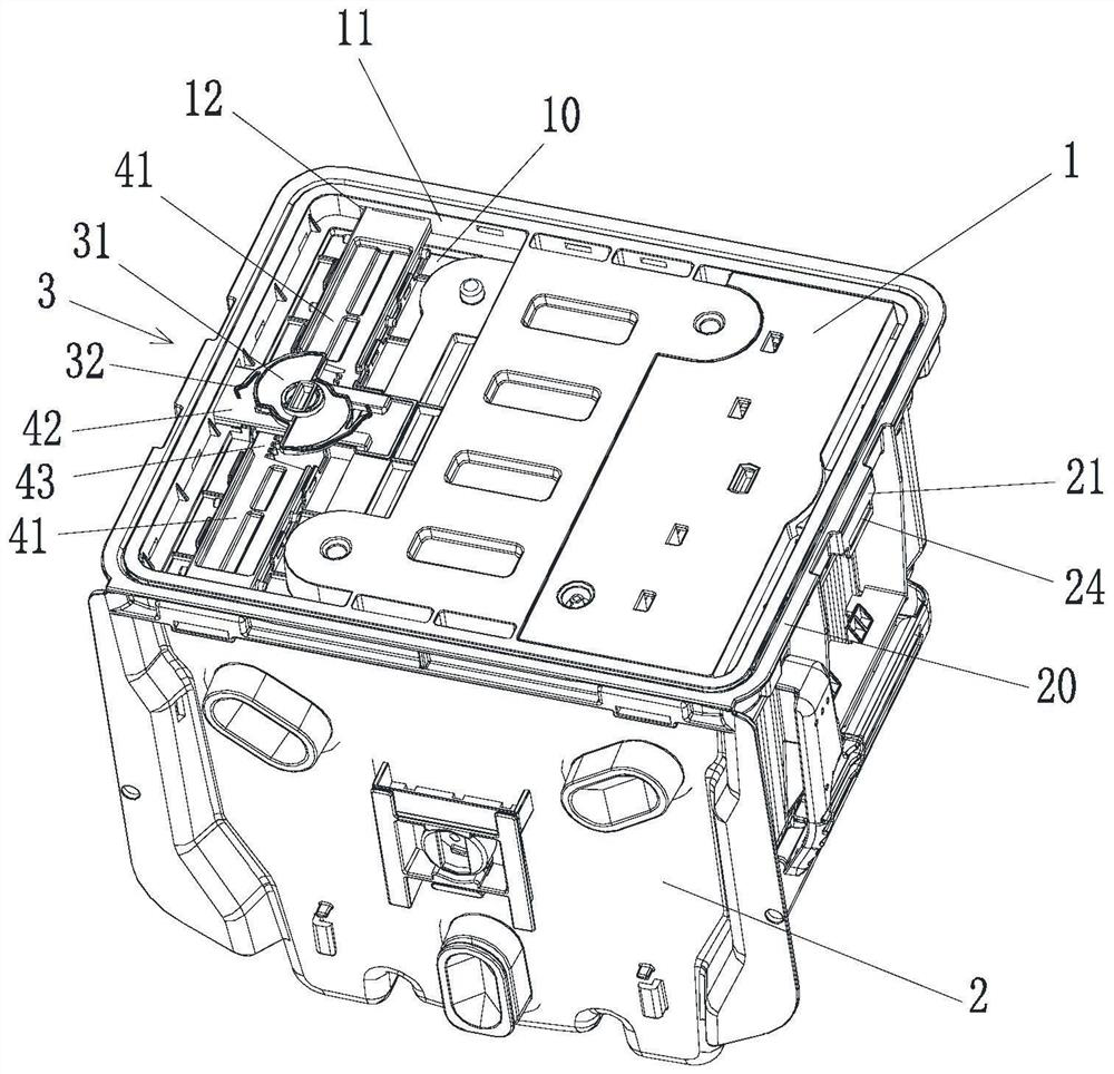
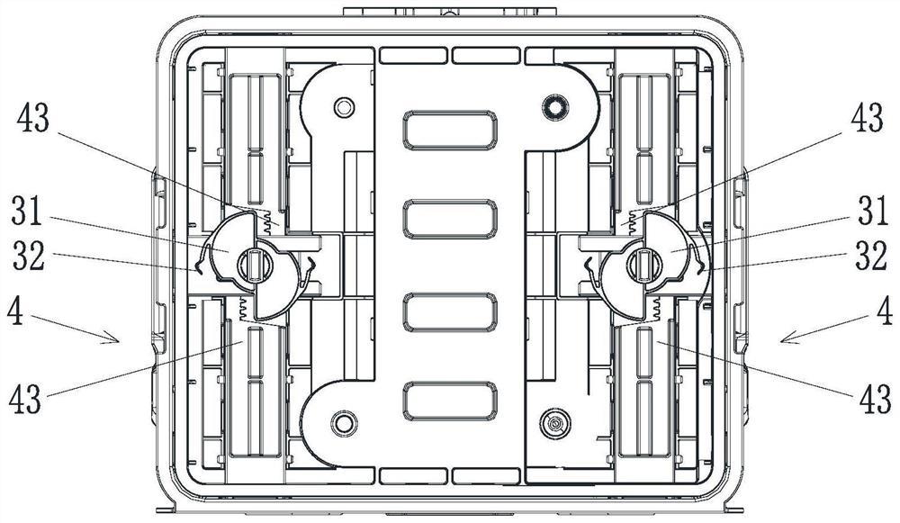
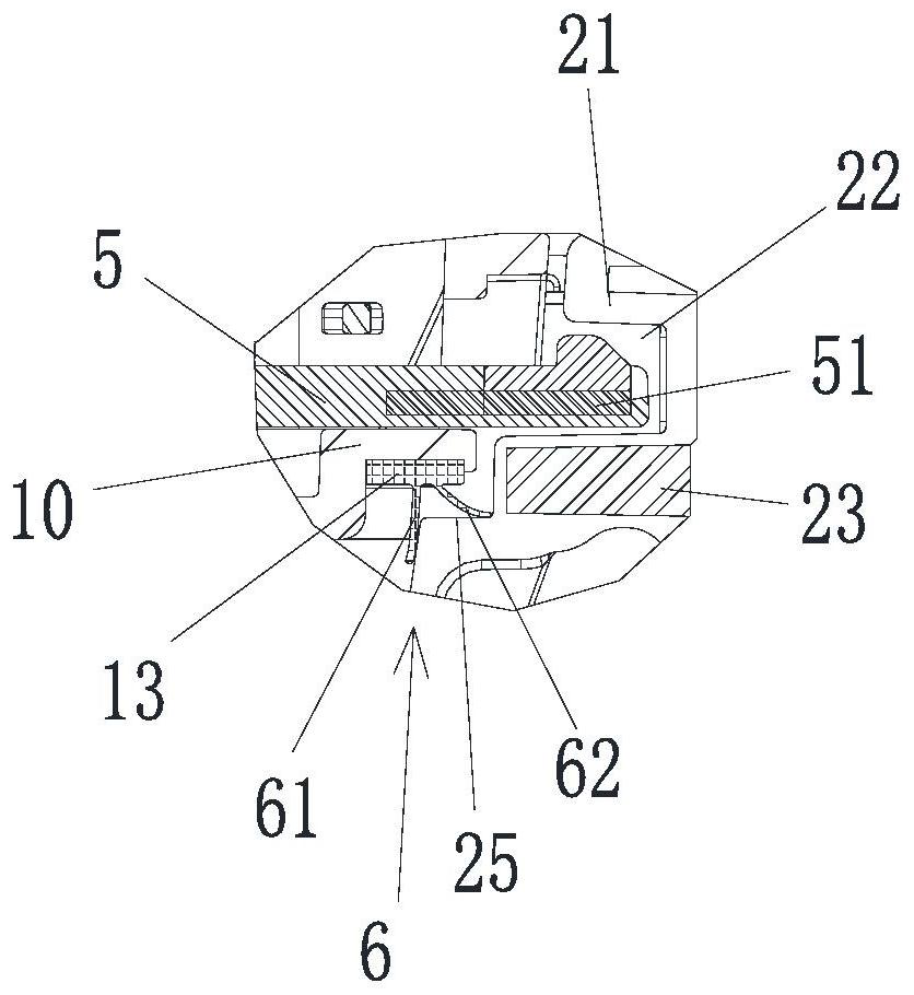
The invention relates to a semiconductor wafer storage container. The semiconductor wafer storage container comprises a container main body and a cover body, the at least one latch mechanism is arranged on the cover body, each latch mechanism comprises a plurality of latch advancing and retreating parts arranged in the circumferential direction of the cover body, and a groove used for containing the latch advancing and retreating parts is formed in the container main body; the flexible rubber strip is arranged in the circumferential direction of the face, facing the container body, of the cover body, the flexible rubber strip comprises a base part annularly arranged in the circumferential direction of the cover body and at least one deformable fin arranged in the circumferential direction of the face, facing the container body, of the base part, and the fins are obliquely arranged towards the outer side of the cover body; and the width is greater than that of the base part. The latch advancing and retreating parts are symmetrically arranged in the circumferential direction of the cover body, so that the circumferential distribution of the locking points between the cover body and the container main body is realized.

Description

technical field [0001] The present application relates to the field of semiconductor technology, and in particular, to a semiconductor wafer storage container. Background technique [0002] Semiconductor wafers go through multiple steps during processing and need to be transported or handled between workstations or processing equipment. Semiconductor wafers are easily damaged by physical contact or shock and static electricity, and semiconductor manufacturing processes are sensitive to contamination by particles or chemicals. Therefore, in order to reduce the harmful effects of contaminants on the wafers, containers have been developed that isolate the wafers from contaminants outside the container. A detachable lid body on the front surface of the opening of the container body, and a locking mechanism for locking / unlocking the lid body fitted on the front surface of the container body. [0003] Traditional seals to SMIF boxes and shipping modules are typically relatively ...

Claims


Application Information

Patent Timeline
Patent Type & Authority Applications(China)
IPC IPC(8): H01L21/673B65D53/00B65D55/14B65D81/20B65D85/30
CPCB65D85/30B65D55/14B65D53/00B65D81/2038H01L21/67373H01L21/67386H01L21/67303
Inventor 刘春峰刘国华孟余红
Owner 荣耀半导体材料(嘉善)有限公司
Learn More