
Semiconductor structure

A semiconductor and transistor technology, applied in the field of gate full ring, can solve problems such as increasing the complexity of semiconductor process

Pending Publication Date: 2022-07-19
TAIWAN SEMICON MFG CO LTD
View PDF0 Cites 0 Cited by
  • Summary
  • Abstract
  • Description
  • Claims
  • Application Information

AI Technical Summary

Problems solved by technology

However, this type of scaling also increases the complexity of the semiconductor manufacturing process

Method used


Image

  • Semiconductor structure
  • Semiconductor structure
  • Semiconductor structure

Examples


Embodiment Construction

[0083] The following disclosure provides many different embodiments or examples for implementing different features of the provided subject matter. Specific examples of components, arrangements, etc. are described below to simplify the present disclosure. Of course, it is only an example and not intended to limit the disclosure. For example, forming a first feature on or over a second feature in the following description may include an embodiment in which the first feature and the second feature are formed in direct contact, or may include an embodiment where the first feature and the second feature are in direct contact. An embodiment in which other feature parts are formed between two feature parts, so that the first feature part and the second feature part are not in direct contact. Additionally, this disclosure reuses reference numerals and / or letters in various instances. This reuse is for simplicity and clarity and does not in itself represent a relationship between th...


PUM


Abstract

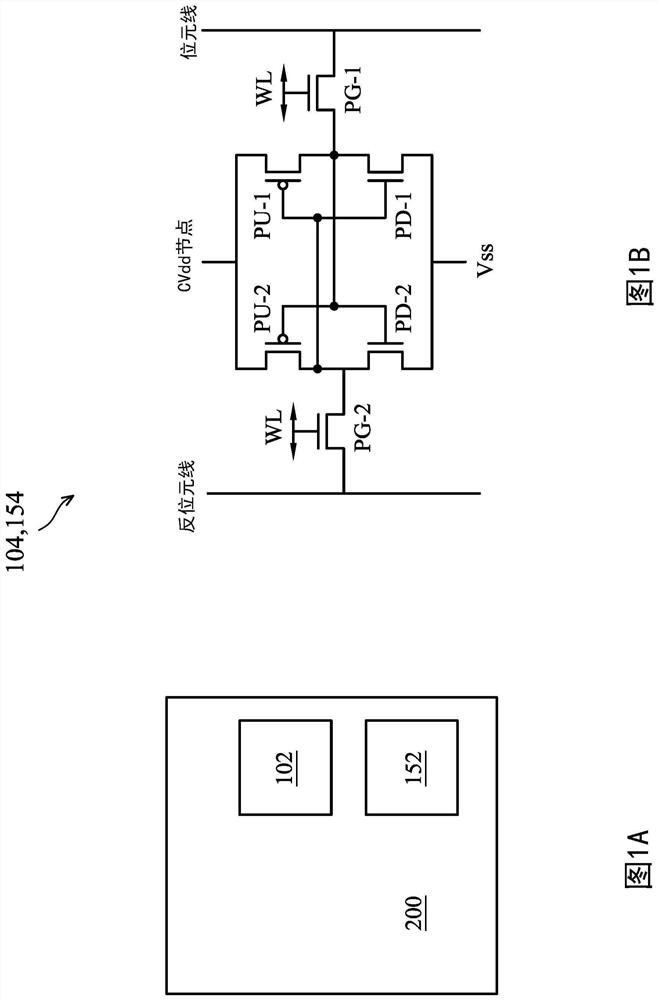
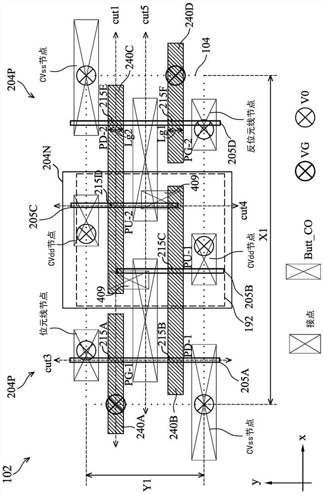
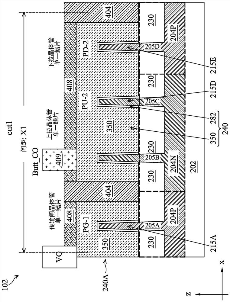
A semiconductor structure includes a substrate, and first and second SRAM cells. Each first SRAM unit comprises two first p type FinFETs (FinFET) and four first n type FinFETs (FinFET); each of the first p-type and first n-type FinFETs includes a channel in a single semiconductor fin. The first SRAM cell has a first X pitch and a first Y pitch. And each second SRAM unit comprises two second p type FinFETs (FinFET) and four second n type FinFETs (FinFET). Each of the second p-type FinFETs includes a channel in a single semiconductor fin. Each of the second n-type FinFETs includes a channel in a plurality of semiconductor fins. The second SRAM cell has a second X pitch and a second Y pitch. The source / drain region of the first p-type FinFET has a higher boron dopant concentration than the source / drain region of the second p-type FinFET. A ratio of the second X-pitch to the first X-pitch is in a range of 1.1 to 1.5.

Description

technical field [0001] The present invention relates to semiconductor structures and processes thereof, and in particular to high-density implementations of fin field effect (FinFET) transistors or gate-all-around (GAA) transistors; HD) memory cells and integrated circuits (ICs) of high-current (HC) (or high-speed (HS)) memory cells. Background technique [0002] The electronics industry faces an increasing demand for smaller and faster electronic devices that simultaneously need to support a large number of increasingly complex and sophisticated functions. To meet this need, a continuing trend in the semiconductor industry is to manufacture integrated circuits (ICs) that are low cost, high performance, and low power. To date, most of these goals have been achieved by reducing the size of semiconductor ICs (eg, IC minimum feature size), thereby improving process efficiency and reducing associated costs. However, such size reductions also increase the complexity of the semi...

Claims


Application Information

Patent Timeline
Patent Type & Authority Applications(China)
IPC IPC(8): H01L27/11H01L21/8244H01L29/78H10B10/00
CPCH01L29/785H10B10/12H01L29/775H01L29/66545H01L29/7848G11C5/025G11C11/412H01L23/5286H01L29/0673H01L29/66439B82Y10/00H01L21/823842H01L21/823807H01L27/0924H01L29/42392H01L29/78696H01L21/823821H10B10/125G11C11/419H01L29/7851H01L29/0847H01L29/4966H01L29/4908H01L29/41733H01L29/78618H01L29/41791H01L21/28088H01L21/823814H01L21/823871H10B10/18
Inventor 廖忠志
Owner TAIWAN SEMICON MFG CO LTD
Learn More