
Device for detecting blocky polycrystalline silicon impurities as well as application and detection method thereof

A technology for polycrystalline silicon and polycrystalline silicon rods is applied in the field of devices for detecting impurities in bulk polycrystalline silicon, which can solve the problems of reduced production cost and high energy consumption, and achieve the effects of improving accuracy, ensuring accuracy, and improving methods that are simple and easy to obtain.

Pending Publication Date: 2022-07-29
江苏鑫华半导体科技股份有限公司
View PDF6 Cites 0 Cited by
  • Summary
  • Abstract
  • Description
  • Claims
  • Application Information

AI Technical Summary

Problems solved by technology

The detection basis of this method is polysilicon rods, which are obtained by the Siemens method, and the relatively high energy consumption of the Siemens method limits the reduction of production costs to a certain extent

Method used


Image

  • Device for detecting blocky polycrystalline silicon impurities as well as application and detection method thereof
  • Device for detecting blocky polycrystalline silicon impurities as well as application and detection method thereof
  • Device for detecting blocky polycrystalline silicon impurities as well as application and detection method thereof

Examples


Embodiment Construction

[0032] The following describes in detail the embodiments of the present invention, examples of which are illustrated in the accompanying drawings, wherein the same or similar reference numerals refer to the same or similar elements or elements having the same or similar functions throughout. The embodiments described below with reference to the accompanying drawings are exemplary, and are intended to explain the present invention and should not be construed as limiting the present invention.

[0033] In the description of the present invention, the terms "first" and "second" are only used for the purpose of description, and cannot be understood as indicating or implying relative importance or implying the number of indicated technical features. Thus, a feature delimited with "first", "second" may expressly or implicitly include at least one of that feature. In the present invention, unless otherwise expressly specified and limited, terms such as "installation", "connection", "...


PUM

PropertyMeasurementUnit
depthaaaaaaaaaa

Abstract

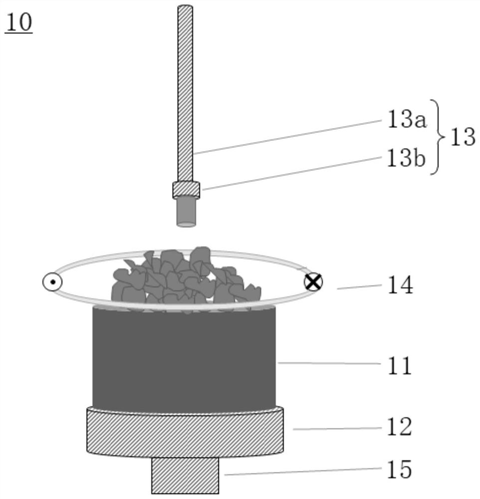
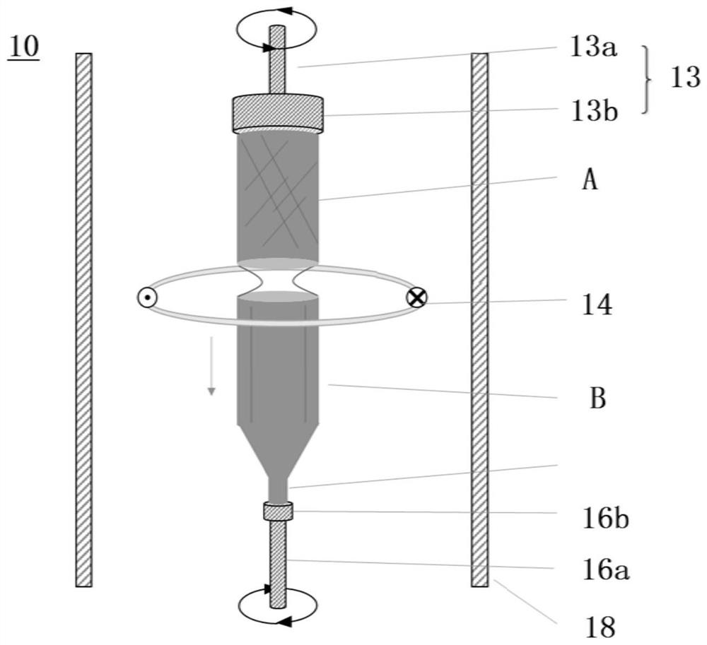
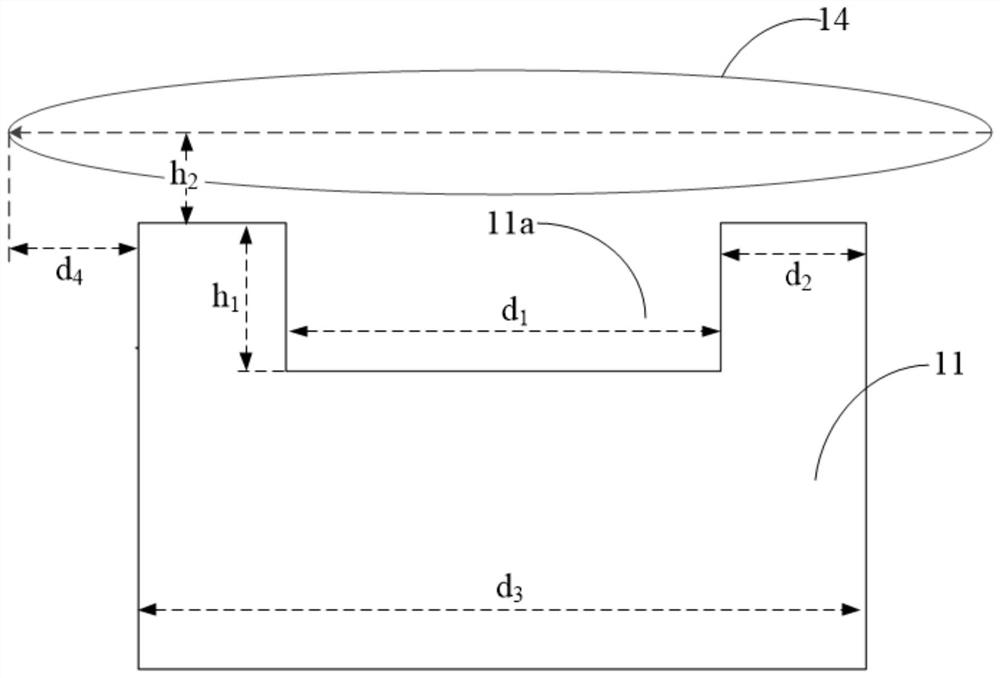
The invention discloses a device for detecting blocky polycrystalline silicon impurities as well as application and a detection method thereof. The device comprises a zone melting furnace, and the zone melting furnace comprises a silicon rod substrate, a silicon rod base, a first seed crystal rotary fixing piece, a heating coil and a rotary supporting part. A groove is formed in the upper part of the silicon rod substrate; the silicon rod base is arranged at the lower part of the silicon rod substrate and supports the silicon rod substrate; the first seed crystal rotary fixing piece comprises a first screw rod and a first seed crystal chuck and is arranged at the upper part of the zone melting furnace; the heating coil is arranged between the first seed crystal rotary fixing piece and the silicon rod substrate, and the projection of the heating coil on the horizontal plane is located outside the projection area of the silicon rod substrate on the horizontal plane; and the rotary supporting part is arranged at the bottom of the zone melting furnace and supports the silicon rod base. The device is simple in structure and convenient to operate, can realize the conversion from the blocky polycrystalline silicon to the polycrystalline silicon rod, further can obtain the impurity content of the blocky polycrystalline silicon by detecting the impurity content of the polycrystalline silicon rod, and has the advantages of high detection result accuracy and easiness in implementation.

Description

technical field [0001] The invention belongs to the technical field of electronic-grade polysilicon, and in particular, relates to a device for detecting impurities in bulk polysilicon, its use, and a detection method. Background technique [0002] Electronic grade polysilicon is the main raw material for manufacturing high-purity silicon products such as solar cells and electronic chips. In the electronic-grade polysilicon industry, the most critical parameter to determine its price and grade is its impurity concentration, namely the three groups (boron B, aluminum Al, gallium Ga and indium In) and five groups (phosphorus P, arsenic) in the periodic table of elements. As and antimony (Sb) and carbon and oxygen impurities. When the impurity content in electronic grade polysilicon is too high, the resistance will decrease, which will affect the resistivity of the single crystal and the lifetime of minority carriers. Therefore, the content of impurities in electronic grade p...

Claims


Application Information

Patent Timeline
Patent Type & Authority Applications(China)
IPC IPC(8): C30B13/00C30B13/20C30B13/28
CPCC30B13/285C30B13/20C30B13/00
Inventor 神干李明峰田新蒋文武张天雨
Owner 江苏鑫华半导体科技股份有限公司
Learn More