FRD device structure manufacturing method

A technology of device structure and manufacturing method, which is applied in semiconductor/solid-state device manufacturing, semiconductor devices, electrical components, etc., can solve the problems of increasing contact resistance and increasing static loss, and achieves reduction of dynamic turn-off loss, reduction of dynamic loss, The effect of lowering the injection efficiency

Pending Publication Date: 2022-07-29
上海埃积半导体有限公司
View PDF0 Cites 0 Cited by
  • Summary
  • Abstract
  • Description
  • Claims
  • Application Information

AI Technical Summary

Problems solved by technology

Generally, the dynamic loss of the FRD device structure can be reduced by reducing the concentration of the front P+ region, such as image 3 The FRD device structure of the prior art shown, but the too low concentration of the P-type region will increase the contact resistance between it and the front anode metal, thereby increasing the static loss

Method used


Image

  • FRD device structure manufacturing method
  • FRD device structure manufacturing method
  • FRD device structure manufacturing method

Examples


Embodiment Construction

[0044] In the following description, for the purpose of illustration rather than limitation, specific details, such as specific system structures and technologies, are provided for a thorough understanding of the embodiments of the present application. However, it will be apparent to those skilled in the art that the present application may be practiced in other embodiments without these specific details. In other instances, detailed descriptions of well-known systems, devices, circuits, and methods are omitted so as not to obscure the description of the present application with unnecessary detail.

[0045] It is to be understood that, when used in this specification and the appended claims, the term "comprising" indicates the presence of the described feature, integer, step, operation, element and / or component, but does not exclude one or more other The presence or addition of features, integers, steps, operations, elements, components and / or collections.

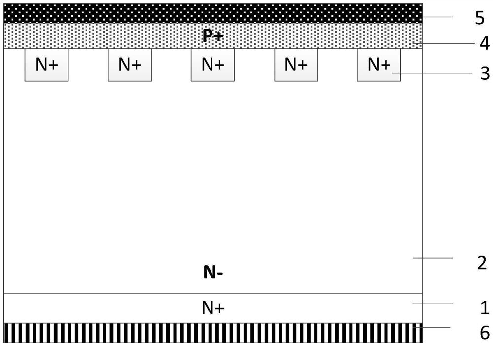
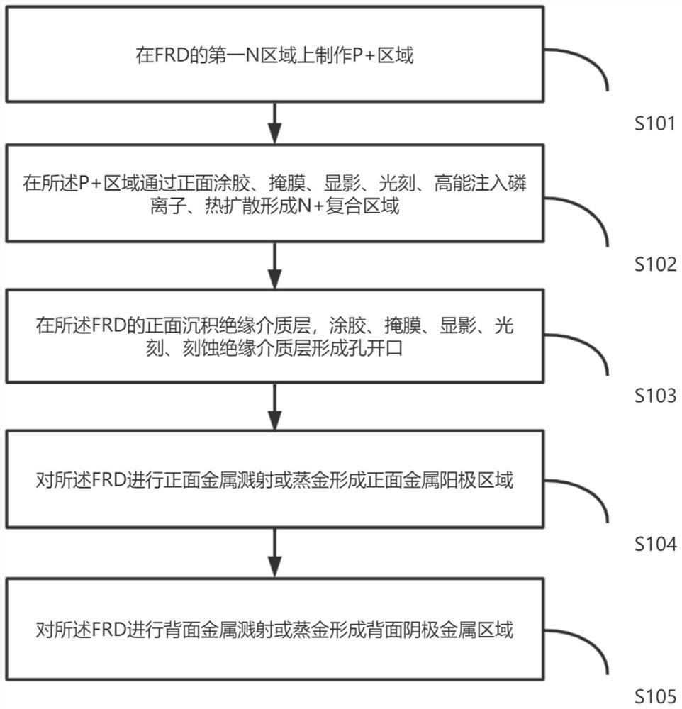
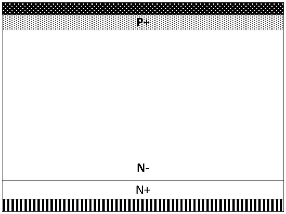
[0046] In order t...


PUM


Abstract

The invention provides an FRD device structure. The FRD device structure comprises a first N region, a P + region, an N + composite region, a front anode metal region and a back cathode metal region, the first N region comprises a first N + region and a first N-region; the first N-region is located above the first N + region; the P + region is located on the first N-region; the N + composite region is located in the first N-region; the front anode metal region is located on the P + region; and the back cathode metal region is located below the first N + region. On the premise of not reducing the concentration of the front P-type region, the N + composite region is introduced to reduce the front hole injection efficiency, so that the dynamic loss of the device is reduced.

Description

technical field [0001] The invention relates to the field of semiconductor power devices, in particular to an FRD device structure and a manufacturing method. Background technique [0002] Fast recovery diode (FRD for short) is a semiconductor diode with good switching characteristics and short reverse recovery time. It is mainly used in switching power supplies, PWM pulse width modulators, frequency converters and other electronic circuits. Freewheeling diodes, etc. are used. [0003] In order to match the application environment of faster and faster circuit switching speed, the FRD device structure must meet the characteristics of fast switching speed and low static and dynamic losses. The dynamic loss of FRD device structures can usually be reduced by reducing the concentration of the front-side P+ region, such as image 3 The prior art FRD device structure is shown, but too low a concentration of P-type region increases the contact resistance with the front-side anode m...

Claims


Application Information

Patent Timeline
Patent Type & Authority Applications(China)
IPC IPC(8): H01L29/868H01L29/06H01L21/329
CPCH01L29/868H01L29/0603H01L29/6609
Inventor 程炜涛姚阳
Owner 上海埃积半导体有限公司
Why Eureka
Try Eureka