Silicon carbide split gate mosfet with integrated high-speed freewheeling diode and preparation method

A freewheeling diode and silicon carbide technology, which is applied in the manufacture of diodes, transistors, semiconductor/solid-state devices, etc., can solve the problems of high conduction voltage drop of SiC body diodes, inability to use freewheeling diodes, and high density of JFET regions. The effect of improving long-term reliability, reducing utilization efficiency, and improving robustness

Active Publication Date: 2022-04-22
NOVUS SEMICON CO LTD
View PDF10 Cites 0 Cited by
  • Summary
  • Abstract
  • Description
  • Claims
  • Application Information

AI Technical Summary

Problems solved by technology

[0004] However, there are two problems in the planar SiC VDMOS. One is that the density of the JFET area is relatively high, which introduces a large Miller capacitance, which increases the dynamic loss of the device; the other is that the conduction voltage drop of the parasitic SiC body diode is too high. , and it is a bipolar device with a large reverse recovery current, so it cannot be used directly as a freewheeling diode

Method used


Image

  • Silicon carbide split gate mosfet with integrated high-speed freewheeling diode and preparation method
  • Silicon carbide split gate mosfet with integrated high-speed freewheeling diode and preparation method
  • Silicon carbide split gate mosfet with integrated high-speed freewheeling diode and preparation method

Examples


Embodiment 1

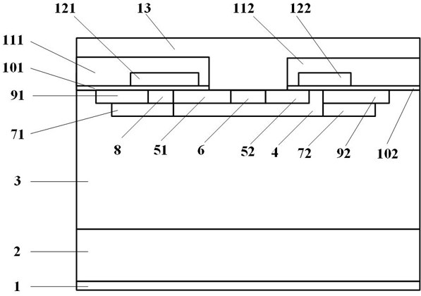
[0048] Such as figure 1 As shown, this embodiment provides a silicon carbide split-gate MOSFET integrating high-speed freewheeling diodes, including a rear ohmic contact alloy 1, an N-type doped silicon carbide substrate 2, an N-type doped silicon carbide epitaxial layer 3, and a P-type silicon carbide epitaxial layer 3. Doped well region 4, first N-type doped source region 51, second N-type doped source region 52, P-type doped source region 6, first P-type doped buried layer 71, second P-type doped source region Buried layer 72, P-type doped diode channel region 8, first N-type doped guide layer 91, second N-type doped guide layer 92, first gate oxide layer 101, second gate oxide layer 102, A first interlayer dielectric 111, a second interlayer dielectric 112, a first polysilicon 121, a second polysilicon 122, and a source metal 13;

[0049] The N-type doped silicon carbide substrate 2 is located above the back ohmic contact alloy 1; the N-type doped silicon carbide epitaxia...

Embodiment 2

[0060] This embodiment provides a method for preparing a silicon carbide split-gate MOSFET integrated with a high-speed freewheeling diode, which includes the following steps:

[0061] Step 1: Epitaxially forming an N-type doped silicon carbide epitaxial layer 3 on an N-type silicon carbide substrate 2; Figure 5 structure;

[0062] Step 2: Form the first barrier layer 21 by chemical vapor deposition on the surface of the N-type doped silicon carbide epitaxial layer 3, and photolithographically form the first barrier layer 21 to form the first ion implantation window 1-1, using high-temperature Al with a temperature greater than 773K Ion implantation forms a P-type doped well region 4; Figure 6 structure;

[0063] Step 3: Form the second barrier layer 22 on the surface of the first barrier layer 21 and the P-type doped well region 4 by chemical vapor deposition, and leave the sidewall of the second barrier layer 22 by etching to form the second ion implantation window 1- 2...


PUM


Abstract

The invention relates to a silicon carbide split-gate MOSFET integrated with a high-speed freewheeling diode and a preparation method thereof, belonging to the technical field of power semiconductor devices. The MOSFET of the present invention adopts the design of the split gate to reduce the switching loss of the device. In order to prevent the gate oxygen reliability problem caused by the split gate structure, a P-type buried layer is added to reduce the electric field intensity of the polysilicon edge gate oxide layer. Furthermore, an N-type conduction layer is added to introduce current from the channel to the drift region of the device. In addition, in order to reduce the turn-on voltage drop of the silicon carbide MOSFET parasitic body diode and introduce a unipolar conduction mode, a high-speed freewheeling diode based on a MOS structure is introduced on the other side of the MOSFET cell. Compared with the traditional method, the present invention The high-speed freewheeling diode uses the surface tailing of the P-type buried layer to form a channel region, that is, the conduction voltage drop of the high-speed freewheeling diode is reduced as much as possible without adding additional versions.

Description

technical field [0001] The invention belongs to the technical field of power semiconductor devices, and in particular relates to a silicon carbide split-gate MOSFET integrated with a high-speed freewheeling diode and a preparation method thereof. Background technique [0002] SiC, a wide bandgap semiconductor material, is an ideal material for preparing high-voltage power electronic devices. Compared with Si materials, SiC materials have a high breakdown electric field strength (4×10 6 V / cm), high carrier saturation drift velocity (2×10 7 cm / s), high thermal conductivity, and good thermal stability, so it is especially suitable for high-power, high-pressure, high-temperature and radiation-resistant electronic devices. [0003] SiC VDMOS is a commonly used device in SiC power devices. Compared with bipolar devices, SiCVDMOS has better frequency characteristics and lower switching losses because it has no charge storage effect. At the same time, the wide band gap of SiC mate...

Claims


Application Information

Patent Timeline
Patent Type & Authority Patents(China)
IPC IPC(8): H01L29/423H01L29/06H01L29/10H01L29/78H01L27/06H01L21/82H01L21/336H01L21/28
CPCH01L27/0629H01L29/7827H01L29/66068H01L21/8213H01L29/401H01L29/42356H01L29/0684H01L29/0696H01L29/1037
Inventor 顾航高巍戴茂州
Owner NOVUS SEMICON CO LTD
Why Eureka
Try Eureka