Silicon optical monolithic integrated chip containing silicon nitride waveguide and preparation method of silicon optical monolithic integrated chip

A monolithic integration, silicon nitride wave technology, applied in the field of integrated optics, can solve problems such as difficult to manufacture modulators, limit the use of silicon nitride-based integrated chips, etc., to achieve improved crosstalk characteristics, improve the maximum input optical power, low Effect of Coupling Loss

Pending Publication Date: 2022-08-09
NANO BEIJING PHOTONICS
View PDF0 Cites 0 Cited by
  • Summary
  • Abstract
  • Description
  • Claims
  • Application Information

AI Technical Summary

Problems solved by technology

However, it is difficult to manufacture high-speed active devices such as modulators and detectors based on silicon nitride materials, which limits the use scenarios of silicon nitride-based integrated chips

Method used


Image

  • Silicon optical monolithic integrated chip containing silicon nitride waveguide and preparation method of silicon optical monolithic integrated chip
  • Silicon optical monolithic integrated chip containing silicon nitride waveguide and preparation method of silicon optical monolithic integrated chip
  • Silicon optical monolithic integrated chip containing silicon nitride waveguide and preparation method of silicon optical monolithic integrated chip

Examples


Embodiment Construction

[0031] The following description and drawings sufficiently illustrate specific embodiments of the invention to enable those skilled in the art to practice them. Other embodiments may include structural, logical, electrical, process, and other changes. The examples are only representative of possible variations. Unless expressly required, individual components and functions are optional and the order of operations may vary. Portions and features of some embodiments may be included in or substituted for those of other embodiments.

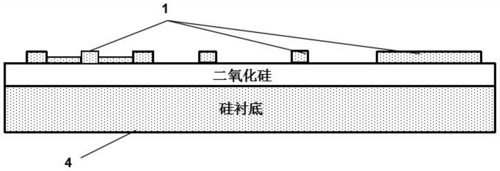
[0032] like figure 1 , 9 , 10, in some illustrative embodiments, the present invention provides a silicon photonics monolithic integrated chip containing a silicon nitride waveguide, the waveguide layer of which is composed of a silicon waveguide 1, a first layer of silicon nitride waveguide 2, and A three-layer optical waveguide composed of the second layer of silicon nitride waveguide 3 .

[0033] The silicon photonics monolithic integrated ch...


PUM


Abstract

The invention provides a silicon optical monolithic integrated chip containing a silicon nitride waveguide. The silicon optical monolithic integrated chip is provided with a silicon waveguide, a first layer of silicon nitride waveguide and a second layer of silicon nitride waveguide. The invention also provides a preparation method of the silicon optical monolithic integrated chip containing the silicon nitride waveguide. The first layer of silicon nitride waveguide is prepared by using a low-pressure chemical vapor deposition method; and the second layer of silicon nitride waveguide is prepared by using a plasma enhanced chemical vapor deposition method. After the silicon nitride waveguide is introduced, the maximum input optical power of the integrated chip, the on-chip loss of the chip and the working temperature range are obviously improved; a single-layer silicon waveguide is increased to three layers of optical waveguides, so that different layers of optical waveguides can be selected to transmit optical signals in an optical waveguide crossing area, the crosstalk characteristic of an integrated chip is remarkably improved, and the integrated chip can be well compatible with a silicon optical active device manufacturing process.

Description

technical field [0001] The invention belongs to the technical field of integrated optics, and in particular relates to a silicon-optical monolithic integrated chip containing a silicon nitride waveguide and a preparation method thereof. Background technique [0002] Although silicon-based photonics integration is regarded as one of the ideal solutions for large bandwidth, low power consumption, and low-cost optical interconnects, silicon photonics integrated chips have certain limitations in performance, such as the two-photon absorption of silicon materials and the free Due to the carrier absorption effect, it is difficult to withstand large optical power, thus limiting the input optical power of the integrated chip; the transmission loss of the silicon optical waveguide is slightly higher, which is easy to cause large on-chip losses of the silicon optical integrated chip, especially for Integrated chips with long routing waveguides and large areas; the thermal-optic coeffi...

Claims


Application Information

Patent Timeline
IPC IPC(8): H01L25/16H01L31/0203H01L31/0232H01L31/18
CPCH01L25/167H01L31/0203H01L31/02325H01L31/18Y02P70/50
Inventor 刘亚东蔡鹏飞苏宗一
Owner NANO BEIJING PHOTONICS
Why Eureka
Try Eureka