Rigid-flex circuit board preparation method and prepared circuit board

A soft-rigid combination, circuit board technology, applied in circuit substrate materials, printed circuit manufacturing, structural connection of printed circuits, etc., to achieve the effect of ensuring stability and ensuring bendability

Pending Publication Date: 2022-08-09
北京大华博科智能科技有限公司
View PDF0 Cites 1 Cited by
  • Summary
  • Abstract
  • Description
  • Claims
  • Application Information

AI Technical Summary

Problems solved by technology

However, for the patch position of components, during the patch welding process, or subjected to continuous bending or stretching deformation, and thermal expansion and contraction of the environment, for example, in the stretched state, the flexible substrate directly below the component is also Tensile deformation occurs, which poses a great challenge to the stability of the components and the integrity of the functions of the components

Method used


Image

  • Rigid-flex circuit board preparation method and prepared circuit board
  • Rigid-flex circuit board preparation method and prepared circuit board

Examples


Embodiment 1

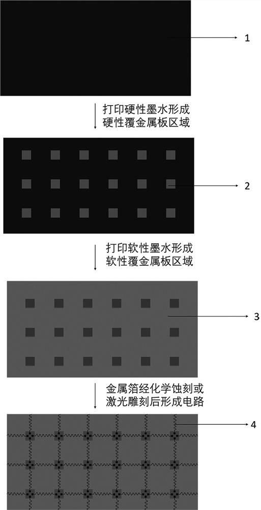
[0026] A method for preparing a single-layer flexible-rigid circuit board, figure 1 It is a schematic diagram of a method for preparing a flexible-rigid circuit board according to Embodiment 1 of the present invention, which includes the following steps:

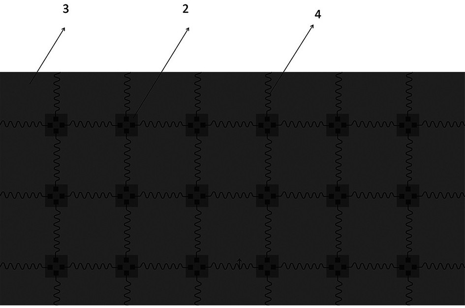
[0027] (1) According to the distribution pattern of the hard area designed by the circuit board, inkjet print the hard ink on the surface of the copper foil 1 and use a 395nm UV lamp to cure; The hard ink and the soft ink are printed on the same side of the copper foil 1.

[0028] (2) After the hard ink of inkjet printing is cured, a rigid metal-clad plate area is formed, and the rigid area is the component bonding and fixing area; the rigid material substrate 2 formed after the hard ink is cured by light is not easily deformed; the softness of inkjet printing After the ink is cured, a flexible metal clad plate area is formed, and the soft area is a circuit conduction area. The flexible material substrate 3 formed by the th...

Embodiment 2

[0033] A method for preparing a multilayer flexible-rigid circuit board, comprising the following steps:

[0034] Make a 3-layer circuit board, each layer of circuit pattern is different, combined into a complete multi-layer circuit board.

[0035] (1) According to the pre-designed hard area distribution pattern of the first layer of circuit board, inkjet print hard ink on the surface of the aluminum foil and use a 365nm UV lamp to cure; The soft ink is inkjet printed and cured by heat; the hard ink and the soft ink are printed on the same side of the aluminum foil.

[0036] (2) The hard ink for inkjet printing forms a hard metal-clad plate area after curing, and the hard area is the component bonding and fixing area; the hard material substrate formed by the hard ink after light curing is not easy to deform; the soft ink for inkjet printing After curing, a soft metal clad plate area is formed, and the soft area is a circuit conduction area. The flexible material substrate fo...


PUM


Abstract

The invention discloses a rigid-flex circuit board preparation method and a prepared circuit board. The method comprises the following steps: (1) according to hard area distribution and soft area distribution designed by a circuit board, respectively printing hard ink and soft ink on the surface of a metal foil in an ink-jet manner; (2) the ink-jet printing hard ink is cured to form a hard metal-clad plate area, and the ink-jet printing soft ink is cured to form a soft metal-clad plate area, so that a soft-hard combined metal-clad plate is formed; and (3) removing unnecessary metal areas based on a chemical etching or laser engraving process, and forming a circuit pattern by the residual metal part, thereby completing the preparation of the single-layer rigid-flex circuit board. In combination with a traditional circuit board manufacturing process, a multi-layer rigid-flex circuit board can be manufactured. According to the technical scheme, the hard part and the soft part of the circuit board can be flexibly designed, the hard part can be used for a fitting area of a component, and the soft part can be used for functions of bending, stretching and the like.

Description

technical field [0001] The invention relates to the technical field of circuit board preparation, in particular to a preparation method of a flexible and rigid circuit board and the prepared circuit board. Background technique [0002] With the rapid development of various medical equipment and various medical detection sensors for health detection, the health status of the body can be detected in real time. In this detection process, many detection sensors need to be in direct contact with the patient's skin, or need to be worn by the patient for a long time. The comfort and use experience of contact or wearing have become urgent requirements for medical electronic equipment or detection sensors. How to develop a skin-like and skin-friendly soft electronic circuit has become a common research and development hotspot in academia and industry. [0003] The skin has the characteristics of softness and stretchability. The preparation of electronic circuits by bionic skin mate...

Claims


Application Information

Patent Timeline
Patent Type & Authority Applications(China)
IPC IPC(8): H05K3/36H05K3/00H05K1/03H05K1/14
CPCH05K3/361H05K3/0011H05K1/147H05K1/03H05K2203/013
Inventor 张兴业
Owner 北京大华博科智能科技有限公司
Why Eureka
Try Eureka