Liquid crystal panel substrate, liquid crystal panel and electronic apparatus using the same

A technology for liquid crystal screens and substrates, which is applied in the direction of identification devices, circuits, transistors, etc., and can solve the problem of not being able to ensure the capacitance value

Inactive Publication Date: 2004-05-12
SEIKO EPSON CORP
View PDF0 Cites 0 Cited by
  • Summary
  • Abstract
  • Description
  • Claims
  • Application Information

AI Technical Summary

Problems solved by technology

[0008] However, if figure 2 As shown in (B), in the conventional example, since the gate electrode 205a and the upper electrode 205b of the storage capacitor are composed of the same layer, the two have to

Method used


Image

  • Liquid crystal panel substrate, liquid crystal panel and electronic apparatus using the same
  • Liquid crystal panel substrate, liquid crystal panel and electronic apparatus using the same
  • Liquid crystal panel substrate, liquid crystal panel and electronic apparatus using the same

Examples


Embodiment Construction

[0046] Hereinafter, preferred embodiments of the present invention will be described with reference to the accompanying drawings.

[0047] (Description of the overall structure of the liquid crystal panel and the structure of the substrate for the liquid crystal panel of the present invention)

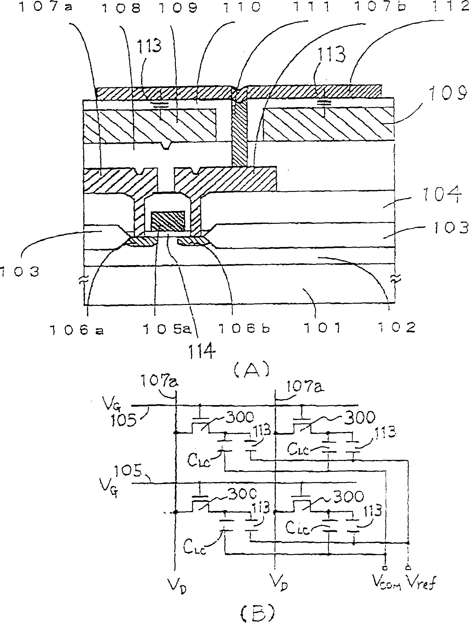
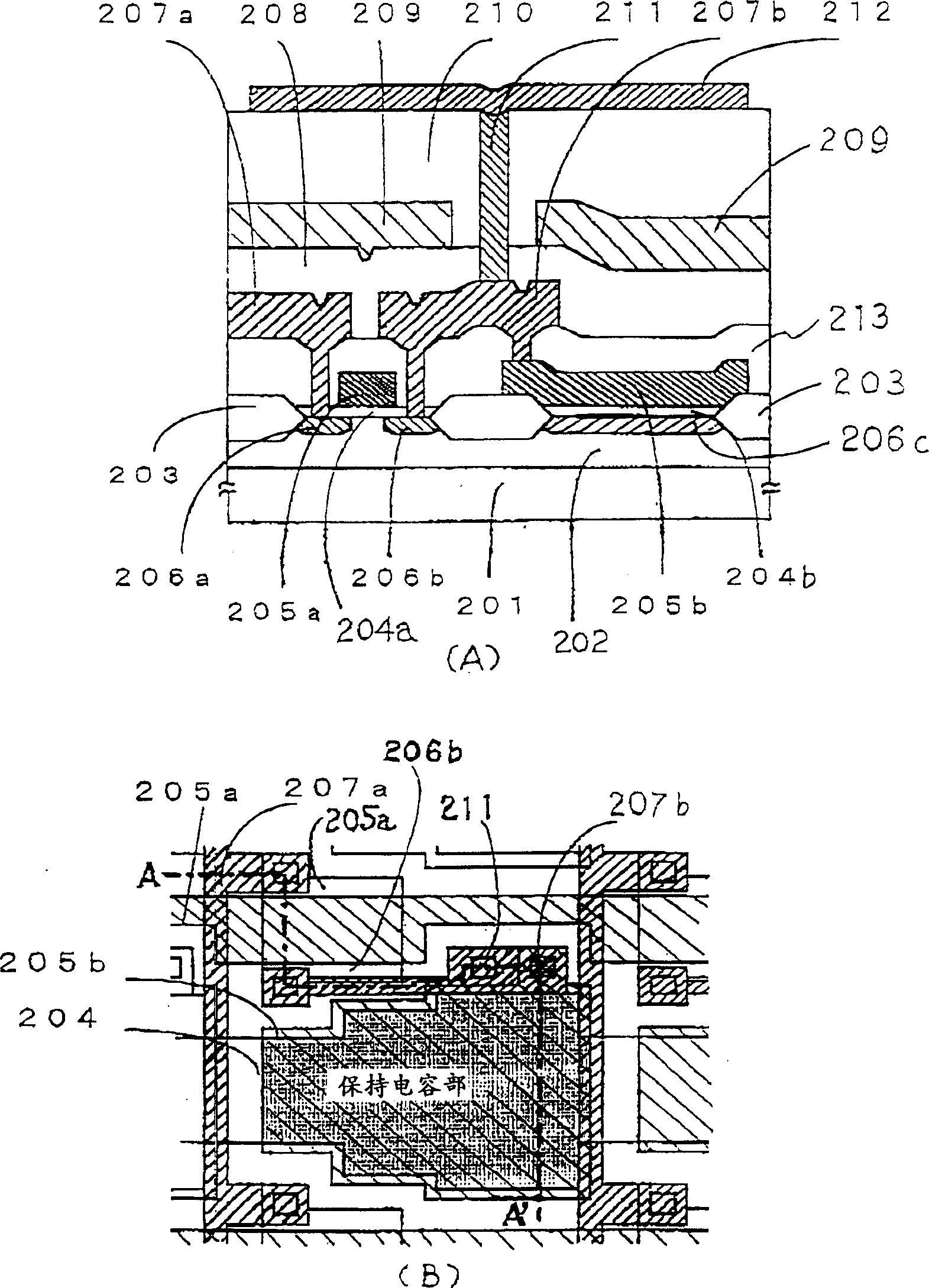
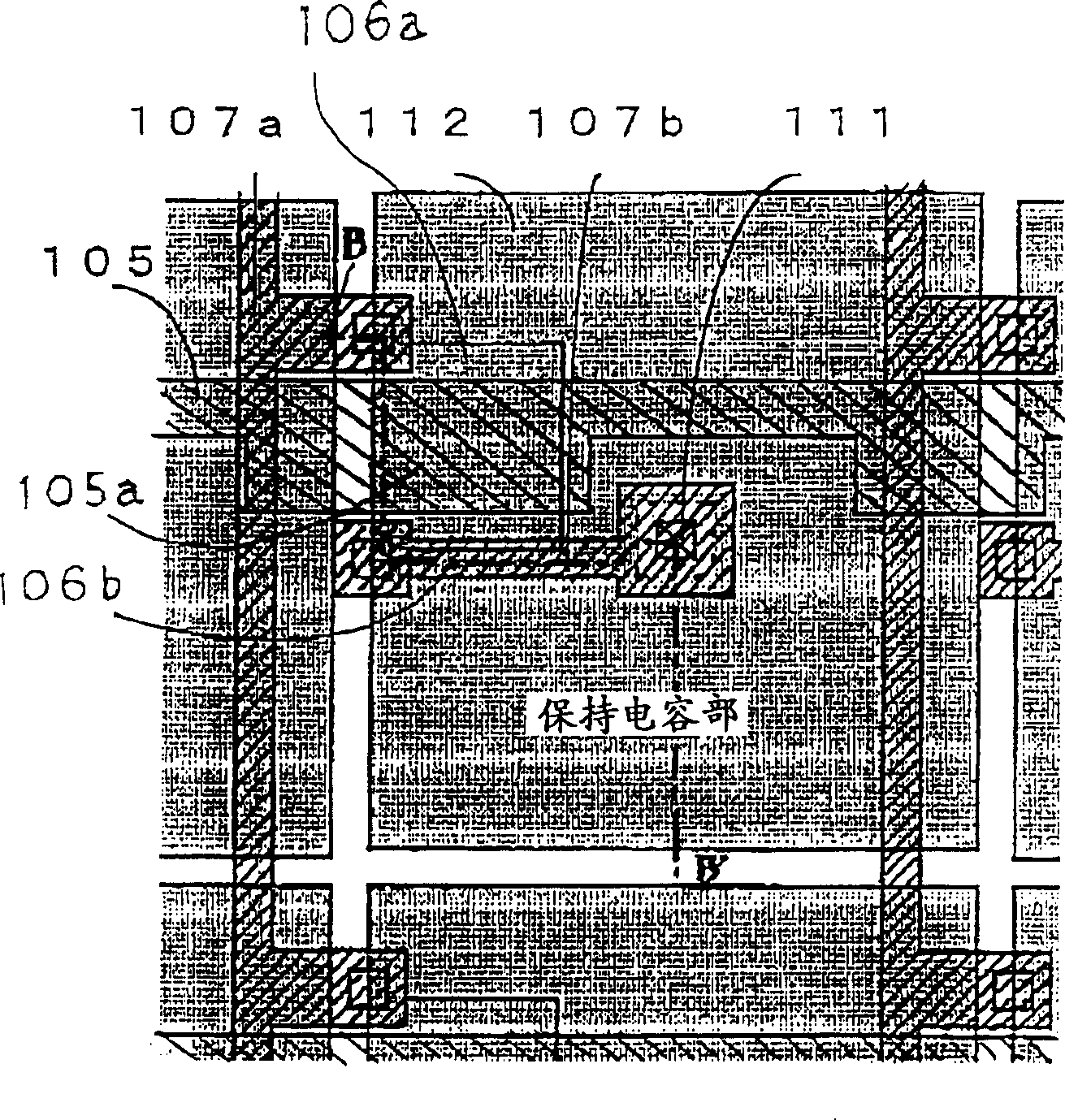
[0048] figure 1 (A) and image 3 It is a cross-sectional view and a plan view showing a first embodiment of the structure of a pixel portion in the pixel region of the reflective electrode side substrate of the reflective liquid crystal panel of the present invention. Figure 15 (A) shows a plan view (A) and a cross-sectional view (B) of the reflective liquid crystal panel of the present invention.

[0049] The reflective electrode side substrate of the present invention is used as figure 1 (A) shows the semiconductor substrate 101 . First, the main part of the overall structure of the reflective liquid crystal panel of the present invention will be described.

[0050] Such as ...


PUM


Abstract

In a conventional reflective liquid crystal panel using a semiconductor substrate, since storage capacitors are formed on the surface of the substrate, with a small pixel size, a sufficient storage capacitor (50 to 100 fF) cannot be ensured, and a voltage necessary for driving a liquid crystal cannot be held. The reflective electrode of each of pixels serves as a conductive layer of one of a pair of electrodes which constitute a storage capacitor, and the other conductive layer of the storage capacitor is formed below the reflective electrode through an insulation film so that the other conductive layer is fixed at the predetermined potential.

Description

technical field [0001] The present invention relates to the structure of a reflective electrode-side substrate constituting a reflective liquid crystal panel, a liquid crystal panel constructed using the substrate, and an electronic device using the liquid crystal panel. Background technique [0002] In the past, as an ultra-small high-definition active matrix liquid crystal panel suitable for applications such as light valves of projectors, a thin-film transistor (TFT) using polysilicon was formed on a quartz substrate, and a pixel electrode was formed on top of it. Transmissive liquid crystal panels made of transparent electrodes have been put into practical use. In the transmissive liquid crystal panel using the above-mentioned TFT, the region of the TFT provided in each pixel and the wiring region constituting the gate electrode, source and drain electrodes for driving the TFT are not the transmissive region through which light is transmitted. As the resolution of the s...

Claims


Application Information

Patent Timeline
IPC IPC(8): G02F1/1343G02F1/133G02F1/136G02F1/1362G02F1/1368G09F9/30H01L21/336H01L29/786
CPCG02F1/136277G02F1/133553G02F1/136213G02F1/136G02F1/1333G02F1/1343
Inventor 片山茂宪
Owner SEIKO EPSON CORP
Why Eureka
Try Eureka