Method for fabricating low-loss optically active device

An active device, optical technology, applied in the direction of optical components, coupling of optical waveguides, instruments, etc., can solve the problems of unfavorable device injection loss, increased total device injection loss, and high optical loss.

Inactive Publication Date: 2004-09-22
SAMSUNG ELECTRONICS CO LTD
View PDF0 Cites 0 Cited by
  • Summary
  • Abstract
  • Description
  • Claims
  • Application Information

AI Technical Summary

Problems solved by technology

Therefore, in the case of forming optical waveguides with the same length and structure, only optical waveguides made of nonlinear optical polymers have the following disadvantages in terms of injection loss of the device compared with optical waveguides formed of linear optical polymers is unfavorable
[0004] Figure 1A and Figure 1B The existing directional coupling optical switch and the existing Mach-Zehnder optical modulator are respectively shown, such as Figure 1A and Figure 1B As shown, since all regions of the optical waveguide including the electrode 130 are composed of nonlinear optical polymers with higher optical losses than linear optical polymers, the total injection loss of the device is significantly increased

Method used


Image

  • Method for fabricating low-loss optically active device
  • Method for fabricating low-loss optically active device
  • Method for fabricating low-loss optically active device

Examples


Embodiment Construction

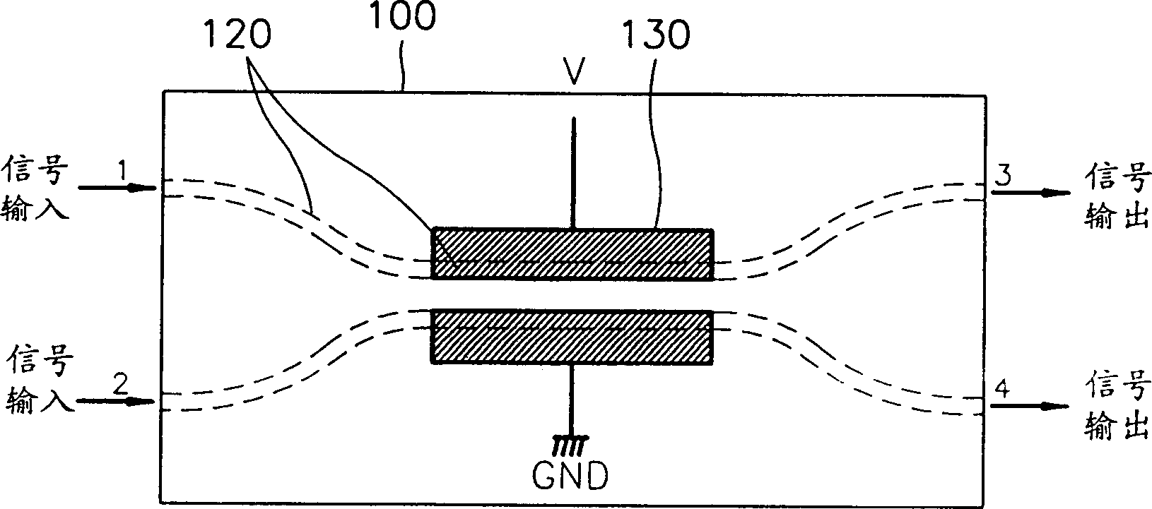
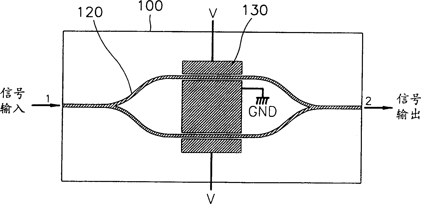
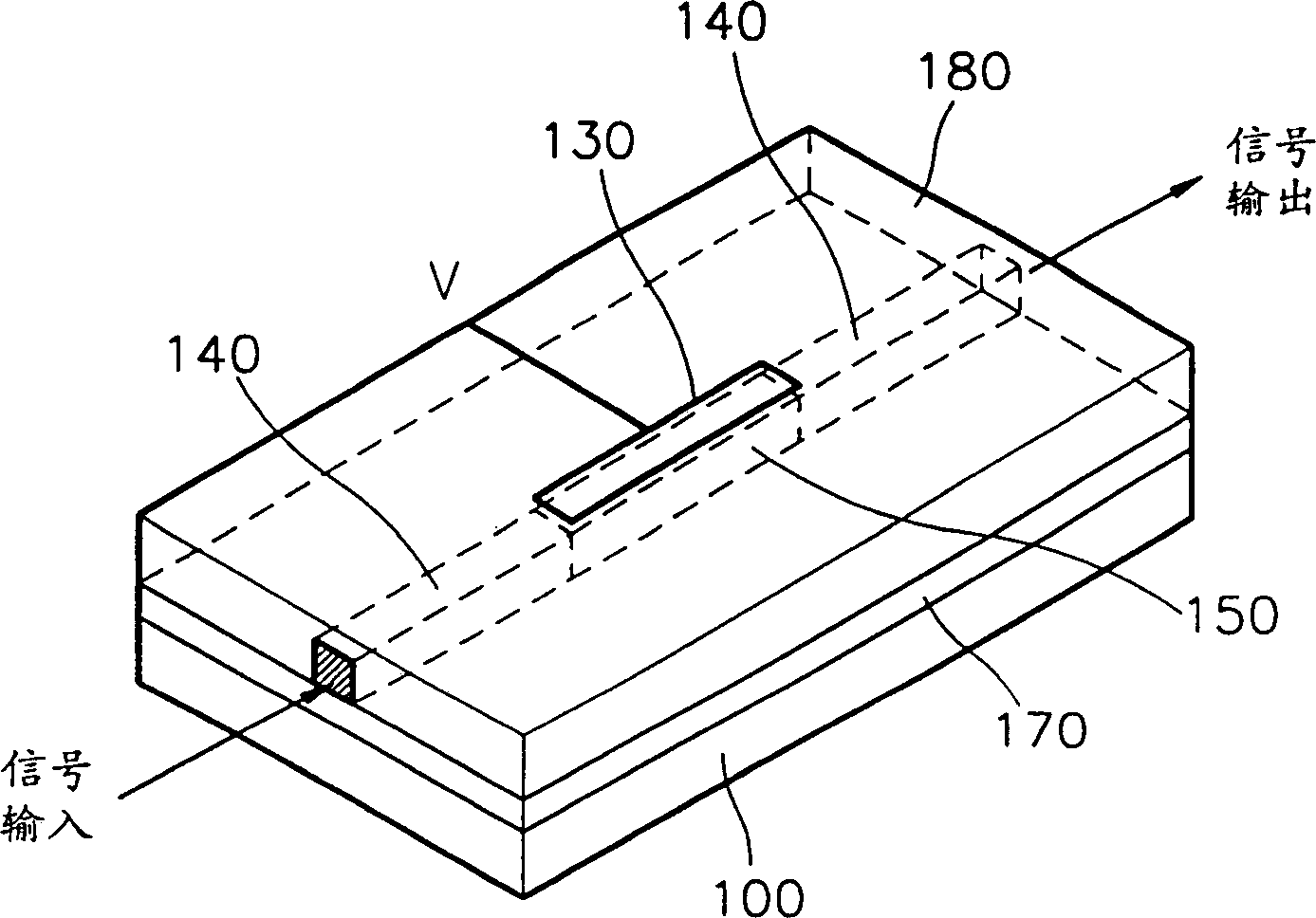
[0029] see figure 2 , the low-loss active device of the present invention is constituted like this: the optical waveguide inner core is made of linear optical polymer and nonlinear optical polymer, the electrode and the optical waveguide inner core that are made of nonlinear optical polymer The formation of regions in the source device where nonlinear interactions occur. The optical active device comprises: a substrate 100; a lower cladding layer 170 arranged on the substrate 100; optical waveguides (140 and 150) for waveguide optical signals arranged on the lower cladding layer 170, which are respectively required non- The nonlinear inner core region 150 of linear action and the linear inner core region 140 that does not require nonlinear action; the upper cladding layer 180 disposed on the optical waveguide (140 and 150) and the lower cladding layer 170; and the nonlinear inner core disposed on electrodes 130 on the area. The nonlinear core region 150 is located between t...


PUM


Abstract

The invention provides a method of manufacturing an optical active device. The optical active device is provided with an optical waveguide which consists of two optical waveguide inner core areas, a nonlinear inner core area which requires nonlinear action and a linear inner core area which does not require the nonlinear action. The method comprises the method of manufacturing the optical active device of the optical waveguide which consists of an optical waveguide inner core area which has the nonlinear action and the optical waveguide inner core area which does not have the nonlinear action. The optical waveguide is formed by nonlinear optical polymer only in the nonlinear action generating area of an optical modulation or an optical switch and is formed by linear optical polymer in other areas, which ensures that the whole waveguide loss of the waveguide is minimized.

Description

technical field [0001] The present invention relates to a method of manufacturing an optical device, in particular to a method of manufacturing a low-loss optical active device by injecting a nonlinear optical polymer only into the region of the optical waveguide where the nonlinear effect occurs to form the inner core of the optical waveguide Reduce the waveguide loss of the device. Background technique [0002] In forming optically active devices such as optical modulators or optical switches using optical polymers, an optical waveguide formed in the device consists of an inner core and upper and lower cladding layers surrounding the inner core. Here, the refractive index of the material used for the inner core is always greater than the refractive index of the material used for the cladding layer. This difference in refractive index causes light passing through the core to propagate along the optical waveguide due to total internal reflection. Traditionally, in fabricat...

Claims


Application Information

Patent Timeline
Patent Type & Authority Patents(China)
IPC IPC(8): G02B6/12G02B6/13G02B26/08G02F1/065G02F1/365
CPCG02F1/365G02F1/065G02B2006/12145G02B2006/12159G02B2006/12147G02B2006/12142G02B2006/12069G02B26/08
Inventor 俞炳权李炯宰李泰衡李勇雨
Owner SAMSUNG ELECTRONICS CO LTD
Why Eureka
Try Eureka