
Inductor device and process of production thereof

A manufacturing method and device technology, applied in the manufacture of inductors/transformers/magnets, inductors, fixed inductors, etc., can solve problems such as complex methods, unfavorable productivity, and increased processes

Inactive Publication Date: 2004-11-24
TDK CORPARATION
View PDF4 Cites 2 Cited by
  • Summary
  • Abstract
  • Description
  • Claims
  • Application Information

AI Technical Summary

Problems solved by technology

[0014] Each of the methods disclosed in the above-mentioned publications adds a process to the prior art ceramic chip stacking method, or makes a significant change
Also, they are more complex than prior art methods and are therefore disadvantageous from a productivity point of view

Method used


Image

  • Inductor device and process of production thereof
  • Inductor device and process of production thereof
  • Inductor device and process of production thereof

Examples


no. 1 example

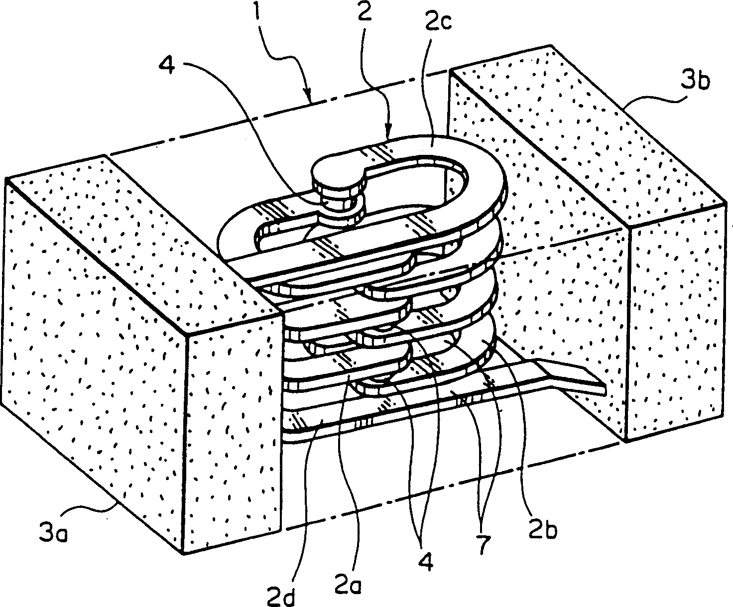
[0044] Such as figure 1 As shown, the inductive device according to the first embodiment has a device body 1 . The device body 1 has terminals 3a and 3b integrally formed at both ends thereof. The device body 1 also has coil pattern units 2 a and 2 b stacked alternately inside the insulating layer 7 . In this embodiment, the end of the coil pattern unit 2c stacked on the top is connected to one terminal 3a, and the end of the coil pattern unit 2d stacked on the bottom is connected to the other terminal 3b. These coil pattern units 2a, 2b, 2c, and 2d are connected via via holes 4 formed in the insulating layer 7, and constitute the coil 2 together.

[0045] The insulating layer 7 constituting the device body 1 is made of, for example, ferrite, ferrite-glass composition, or other magnetic materials, or alumina-glass composition, crystallized glass, or other dielectric materials. The coil pattern units 2a, 2b, 2c and 2d are composed of, for example, silver, palladium, alloys t...

no. 2 example

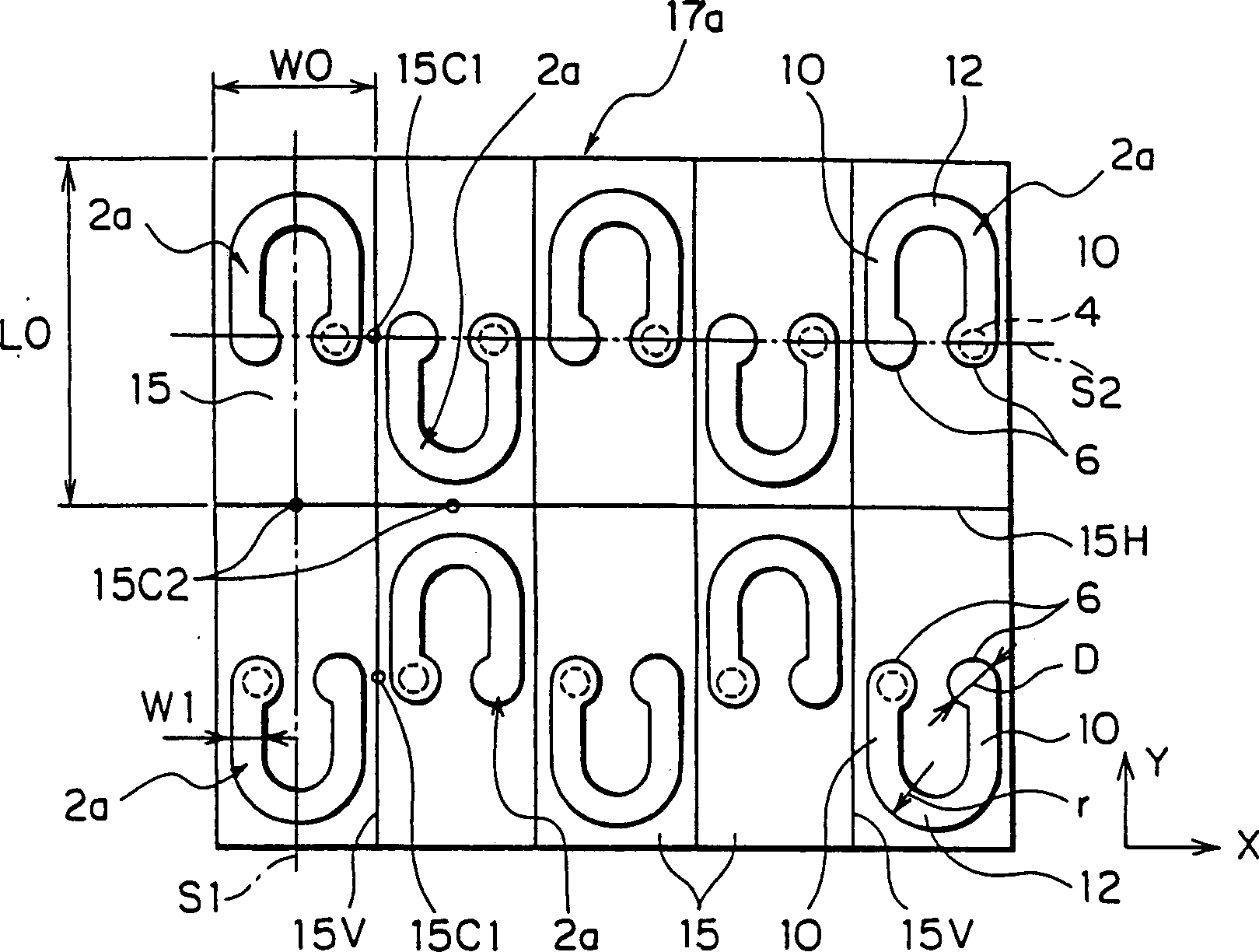
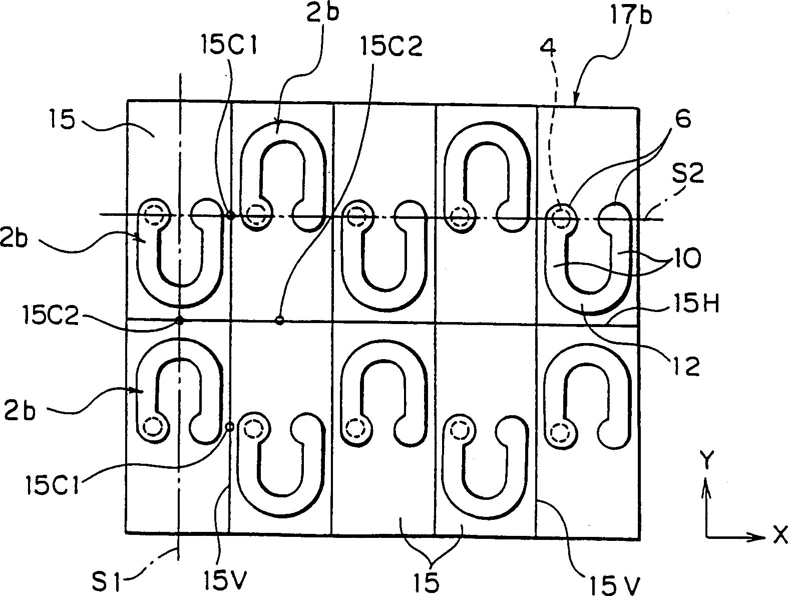
[0067] Such as Figure 4A with 4B As shown, in the manufacturing method of the inductance device according to the second embodiment, the pattern shapes of the coil pattern units 2a' and 2b' themselves formed inside the unit segments 15 of the green sheets 17a and 17b are different from those according to the first embodiment The pattern shapes of the coil pattern units 2a and 2b are the same, but the pattern configurations are different. That is, in the present invention, if Figure 4A with 4B As shown, every two coil pattern units 2a' and 2a' (or 2b' and 2b') adjacent to each other in the longitudinal direction Y of the unit segment 15 are based on the center point 15C2 of the horizontal boundary line 15H of the adjacent unit segment 15. Centrosymmetric graphic configuration. That is, in this embodiment, every two coil pattern units 2 a ′ and 2 a ′ (or 2 b ′ and 2 b ′) adjacent to each other in the longitudinal direction Y of the unit segment 15 are arranged at the same p...

no. 3 example

[0073] In the inductance array device (type of inductance device) according to the third embodiment, such as Image 6 As shown, a plurality of coils 102 are arranged inside a single device body 101 along the longitudinal direction of the device body 101 . A plurality of terminals 103 a and 103 b are formed at side ends of the device body 101 corresponding to the coil 102 .

[0074] Image 6 Shown: the inductance array device of the present embodiment and figure 1 The difference of the shown inductance device is that a plurality of coils 102 are formed inside the device body 101, but the configuration of the coils 102 is the same as figure 1 The coils shown are the same, exhibiting the same process of operation and benefits.

[0075] Image 6 The fabrication method of the inductor array device shown is almost the same as figure 1 The inductor devices shown are manufactured in exactly the same way, except that they are stacked and then diced Figure 2A with 2B Green sheet...


PUM

PropertyMeasurementUnit
Thicknessaaaaaaaaaa
Lengthaaaaaaaaaa
Lengthaaaaaaaaaa

Abstract

A process for the production of an inductor device comprising the steps of forming a green sheet to form an insulating layer; forming a plurality of conductive coil pattern units on the surface of the green sheet in order that a plurality of unit sections each including a single coil pattern unit are arranged on the surface of the green sheet and each two coil pattern units adjoining in the substantially perpendicular direction to the longitudinal direction of the unit sections are arranged centro-symmetrically with respect to a center point of a boundary line of adjoining unit sections; stacking a plurality of green sheets formed with the plurality of coil pattern units arranged in centro-symmetry and connecting the upper and lower coil pattern units separated by the green sheets to form a coil shape; and sintering the stacked green sheets. It is possible to obtain an inductor device able to suppress the stack deviation without complicating the production process even if the device is made small in size.

Description

technical field [0001] The present invention relates to an inductance device and a manufacturing method thereof. Background technique [0002] The market has been demanding smaller electronic devices. There is therefore a need for devices used in electronic equipment to be more compact. Electronic devices that originally had leads have developed into so-called "chip devices" without leads, and at the same time have the advantages of surface mount technology. Capacitors, inductors, and other devices mainly composed of ceramics are manufactured using a chip process based on thick film formation technology or using screen printing technology, etc., and using a co-firing process of ceramics and metals. This enables the realization of a monolithic structure with an inner conductor and allows further size reduction. [0003] The following manufacturing method is suitable for manufacturing such a chip inductor device. [0004] First, ceramic powder is mixed with a solution cont...

Claims


Application Information

Patent Timeline
IPC IPC(8): H01F41/02H01F17/00H01F41/04
CPCH01F41/043H01F17/0013Y10T29/49073Y10T29/49078Y10T29/49069Y10T29/4902H01F41/02
Inventor 安保敏之内木场文男
Owner TDK CORPARATION
Learn More