LED with asymmetrical resonance tunnels

An asymmetric and tunneling technology, applied to the structure of the active region, nano optics, electrical components, etc., can solve problems that hinder the manufacture of high-efficiency LED devices

Inactive Publication Date: 2005-02-02
ARIMA OPTOELECTRONICS
View PDF0 Cites 0 Cited by
  • Summary
  • Abstract
  • Description
  • Claims
  • Application Information

AI Technical Summary

Problems solved by technology

Therefore, the fabrication of high-efficiency LED devices is hampered

Method used


Image

  • LED with asymmetrical resonance tunnels
  • LED with asymmetrical resonance tunnels
  • LED with asymmetrical resonance tunnels

Examples


Embodiment Construction

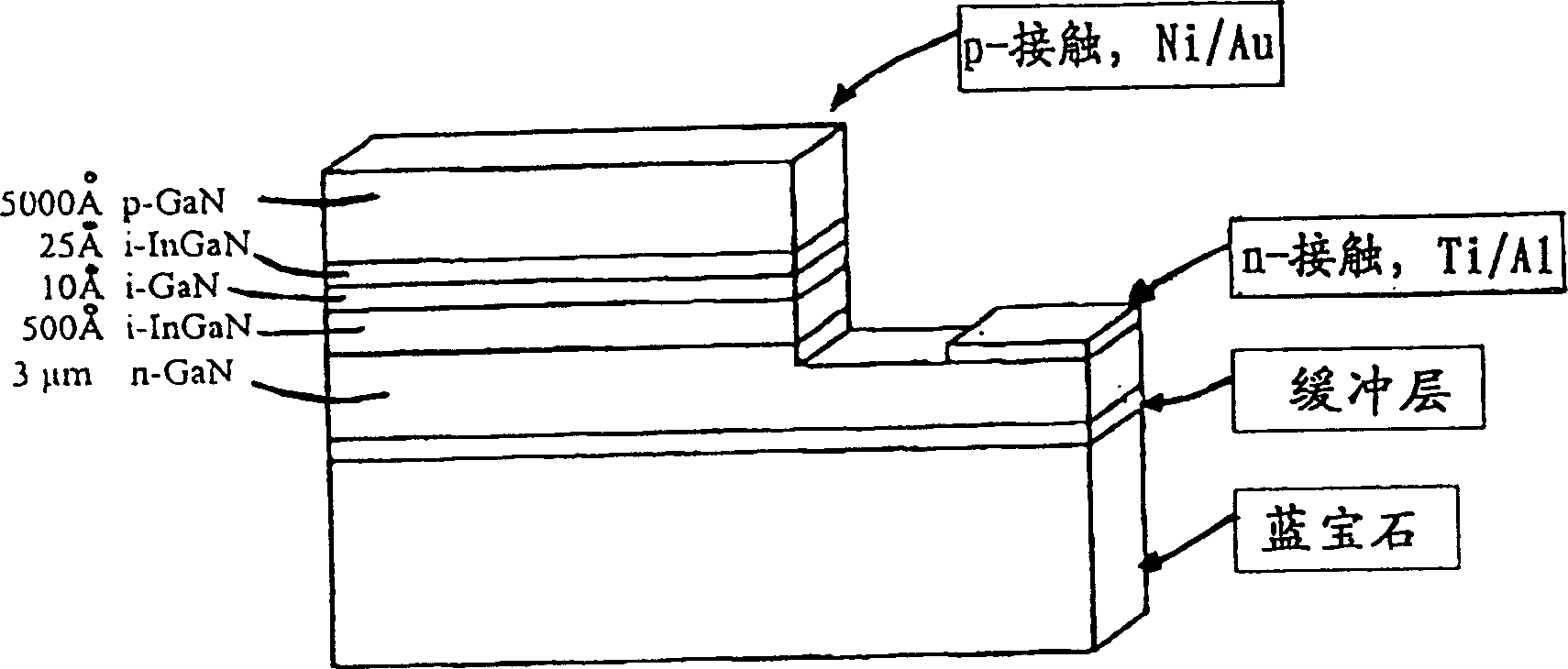
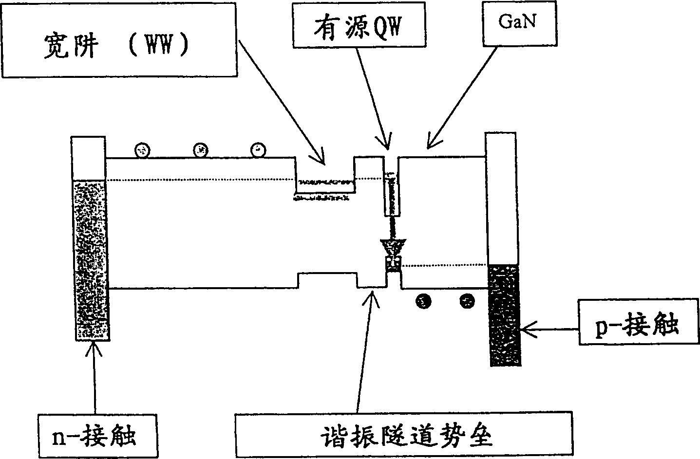
[0026] figure 1 The first structure is shown, which is a GaN blue LED design based on a double well system with asymmetric tunneling. The system includes two coupled wells: a wide well (WW) and an active quantum well (QW). These wells are coupled by a resonant tunnel barrier (RTB) that transmits electrons but blocks holes. Table 1 lists the parameters of the blue LED based on the first structure. Table 2 lists the parameters of the green LED based on the first structure.

[0027] #

[0028] #

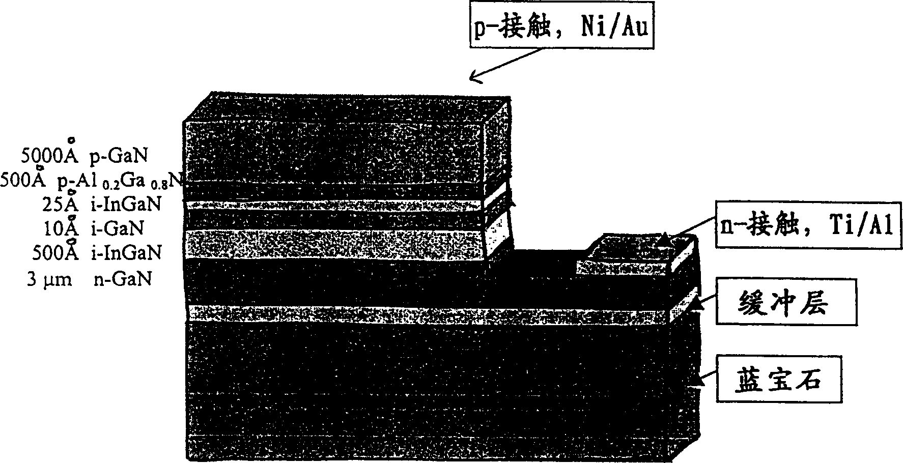
[0029] image 3 A second structure similar to the first is shown, but with additional p-Al 0.1 Ga x-0.1 N electron blocking layer for further reducing electron flow leakage.

[0030] Figure 5 A third structure similar to the second structure is shown, but without the p-GaN layer.

[0031] p-Al 0.1 Ga x-0.1 The N electron blocking layer serves as a contact. This will reduce the thickness of the p-type layer, facilitate the injection of holes into t...


PUM


Abstract

A LED based on dual trap system with charges unbalanced resonance tunnels includes the first and the second couplied traps, one being wide trap and another being active quantum trap. They are coupled via the potential barrier through which to electrons can pass but cavities can not.

Description

technical field [0001] The present invention relates to light emitting diodes (LEDs). Background technique [0002] Semiconductor LEDs emitting red, green, blue, infrared, and ultraviolet light have been on the market for many years. To generate light in LEDs, the radiative recombination of electrons and holes in the active layer is used. The active layer can be a common p-n junction, heterojunction, single quantum well or multiple quantum wells. In some LEDs, single quantum wells or multiple quantum wells are used as the active layer. In order to manufacture high-efficiency devices, the number of carriers recombined in the active layer should be maximized, while the number of carriers recombined outside the active layer should be minimized. This requires optimizing the capture efficiency of electrons and holes into the active layer. In semiconductors, the effective mass of holes is generally larger than that of electrons, while the mobility is much smaller than that of ...

Claims


Application Information

Patent Timeline
Patent Type & Authority Patents(China)
IPC IPC(8): H01L33/06H01L33/32
CPCH01L33/32H01L33/06B82Y20/00
Inventor 王望南优利・G・施里特优利・T・里班
Owner ARIMA OPTOELECTRONICS
Why Eureka
Try Eureka