
Mother electric device, its producing method and electronic device and its producing device

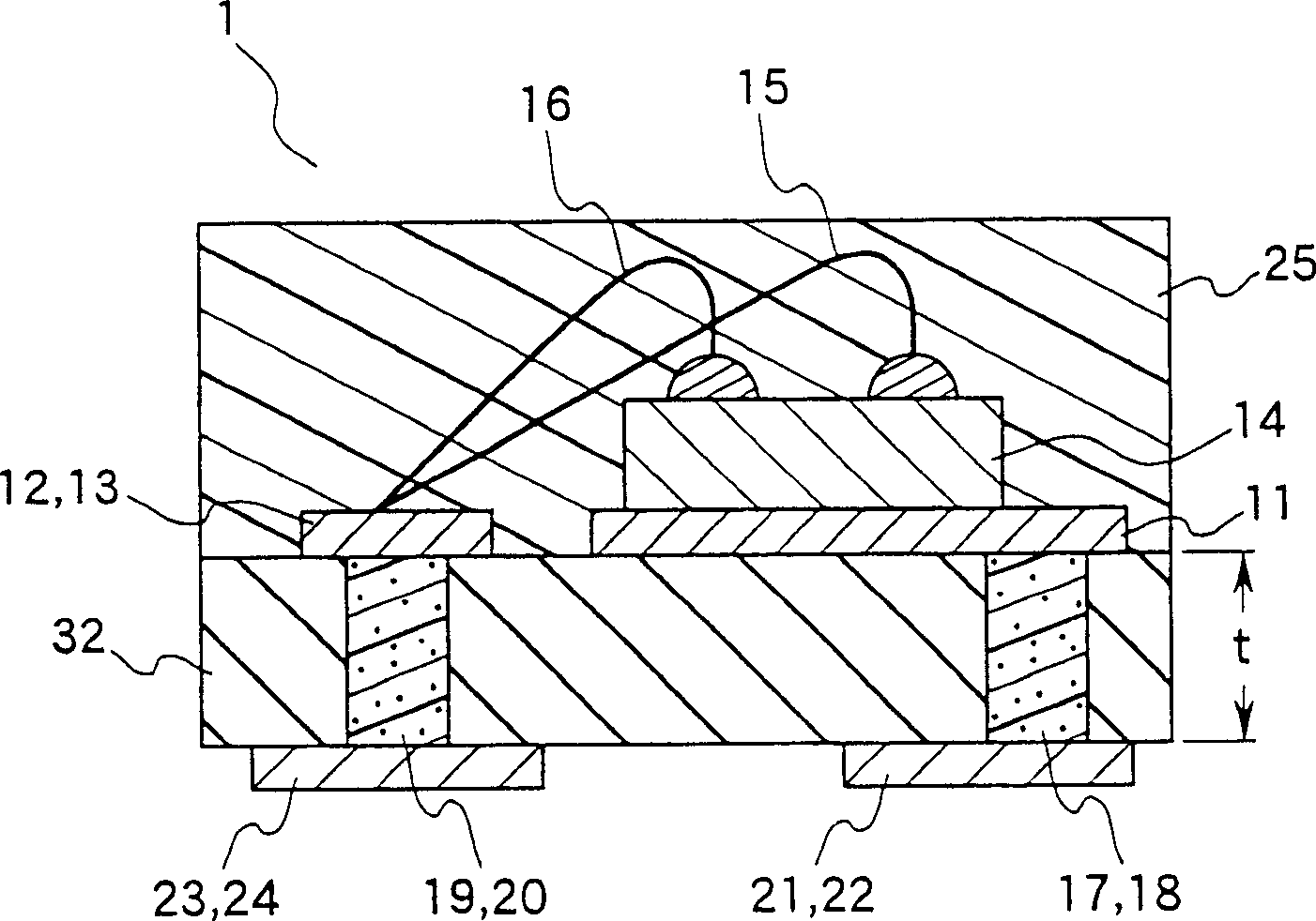
A technology for electronic devices and manufacturing methods, which is applied in the direction of assembling printed circuits with electrical components, semiconductor/solid-state device manufacturing, and printed circuits connected with non-printed electrical components, which can solve the problem of cracks or cracks easily occurring on ceramic substrates, electronic Problems such as device detachment and easy loss

Inactive Publication Date: 2005-07-20
コラボイノベーションズインコーポレイテッド
View PDF0 Cites 0 Cited by
  • Summary
  • Abstract
  • Description
  • Claims
  • Application Information

AI Technical Summary

Problems solved by technology

[0016] In addition, even in the dicing process for forming individual packages, it is difficult to attach the electronic device to the tape for fixing the resin surface due to the unevenness d1 and d2 on the surface of the electronic device after the resin has hardened. There is also the problem that the above-mentioned electronic devices that are cut into individual pieces when cutting are separated from the fixing band and are easily lost.
[0017] In addition, since ceramic substrates are difficult to bend compared to other resin substrates or metal lead frames, cracks are likely to occur in ceramic substrates due to deformation caused by pressure applied when clamping the ceramic substrates with upper and lower metal molds or cracks, so in the conventional non-lead small surface mount type transistors, resin encapsulation by the transfer molding method using the metal mold known so far as the encapsulation method of semiconductors has not been adopted.

Method used


Image

  • Mother electric device, its producing method and electronic device and its producing device
  • Mother electric device, its producing method and electronic device and its producing device
  • Mother electric device, its producing method and electronic device and its producing device

Examples


Embodiment Construction

[0035] In the electronic device of the present invention, the metal thin film is preferably present on both the front side and the back side of the ceramic substrate. This is because the load pressure of both the upper mold and the lower mold can be buffered.

[0036] In addition, in the electronic device of the present invention, it is preferable that the metal thin film and the ceramic substrate are integrally sintered when the metal paste is printed on the green sheet as the raw material of the ceramic substrate and the green sheet is sintered. . This is because cost reduction can be aimed at. Furthermore, it is preferable from the viewpoint of cost that the metal paste is formed in the same process using the same material as the electrode formed on the surface and / or the back surface of the ceramic substrate. For the metal thin film, for example, tungsten can be used.

[0037] In addition, the thickness of the metal thin film is preferably in the range of 10 to 50 µm. ...


PUM

PropertyMeasurementUnit
Thicknessaaaaaaaaaa
Thicknessaaaaaaaaaa
Widthaaaaaaaaaa

Abstract

An electronic device such as a semiconductor device, a method of manufacturing the same, and an apparatus for manufacturing the same, wherein by placing a ceramic substrate (32) provided with a metallic thin film (2) integrated into at least one selected from an upper surface and a lower surface of the ceramic substrate (32) in its peripheral portion so as to extend both inside and outside a cavity (38) of a mold for transfer molding, and positioning the metallic thin film (2) in a position with which an upper mold (30) and a lower mold (31) of the mold come into contact, occurrence of cracks or breakage in the ceramic substrate is prevented by buffering the pressure applied to the ceramic substrate so as to prevent a distortion force from being caused even when the ceramic substrate is sandwiched and compressed between the upper mold and the lower mold.

Description

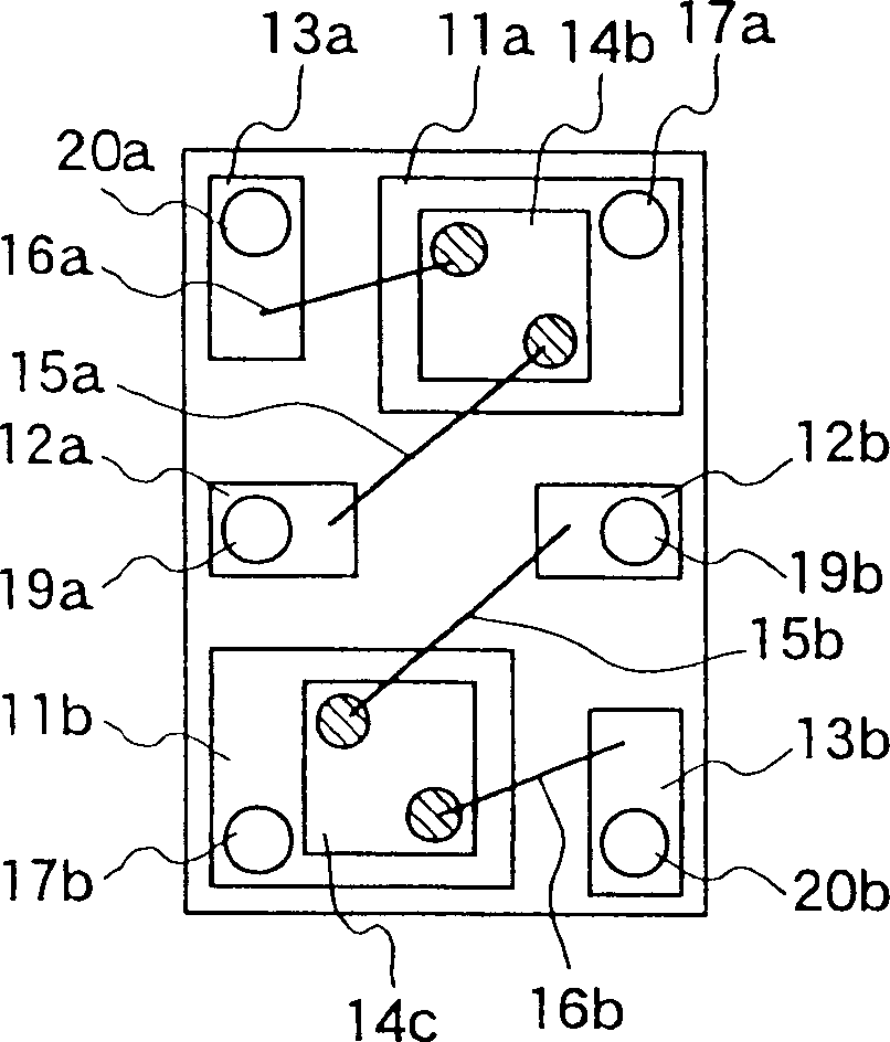
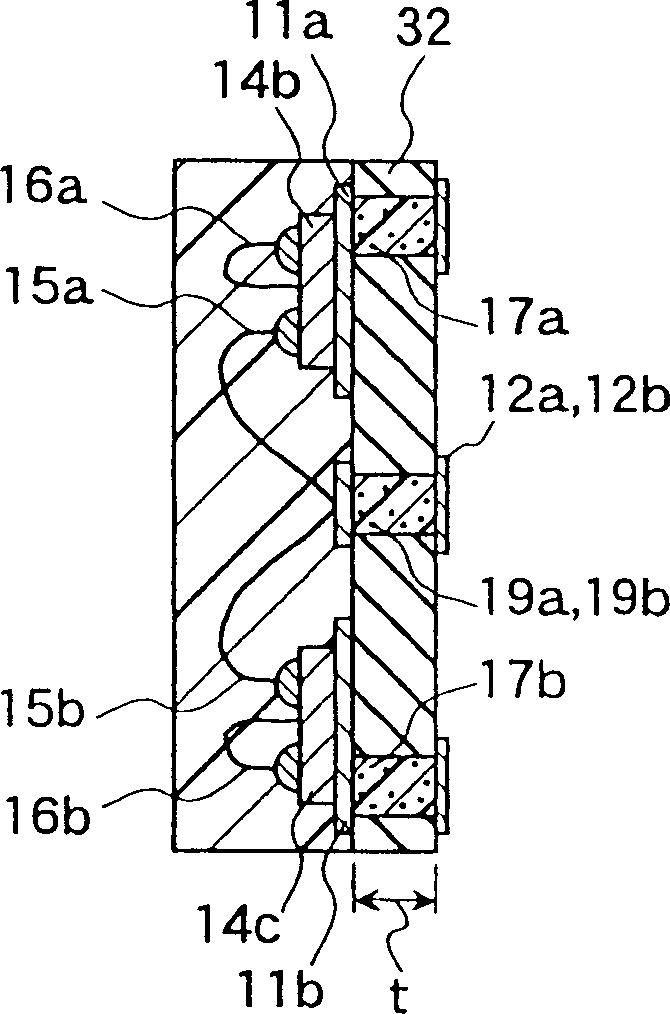
technical field [0001] The present invention relates to an electronic device, a manufacturing method thereof, and a manufacturing device thereof, for example, an electronic device related to a semiconductor device such as a leadless small surface mount type transistor or a diode, a manufacturing method thereof, and a manufacturing device thereof. Background technique [0002] 9A to 9C show structural examples of conventional leadless small surface-mount transistors. That is, FIG. 9A is a plan view of a conventional leadless small surface mount transistor, FIG. 9B is a perspective side view of FIG. 9A, and FIG. 9C is a bottom view of FIG. 9A. [0003] As shown in FIGS. 9A to 9B , the leadless small surface-mount electronic device 3 has: a first upper electrode 11 having an element placement portion on an upper surface 321 of a ceramic substrate 32; and a second upper electrode 12 and a second upper electrode 11. 3. The upper electrode 13 is arranged separately from the first...

Claims


Application Information

Patent Timeline
IPC IPC(8): H01L23/28H01L21/56H01L23/13H01L23/31H01L23/498
CPCH01L24/97H01L2924/15787H01L23/3121H01L2924/01082H01L2924/19043H01L2924/01004H01L2924/01079H01L24/48H01L2224/48465H01L21/561H01L2224/97H01L2924/30105H01L2224/48227H01L2924/14H01L2924/01033H01L2924/01009H01L2924/01005H01L2924/01006H01L24/49H01L2924/01074H01L2924/01078H01L2224/48091H01L2924/01087H01L2224/49171H01L23/49838H01L21/565H01L2224/451H01L2924/181H01L2924/00014H01L24/45H01L2224/85H01L2924/00H01L2924/00012H01L2924/00015H01L2224/05599
Inventor 小林健荒木隆志
Owner コラボイノベーションズインコーポレイテッド
Learn More