Supercharge Your Innovation With Domain-Expert AI Agents!

LCD device with address mark connected with wiring

A technology of address marking and liquid crystal display, applied in instruments, nonlinear optics, optics, etc., can solve problems such as melting and address marking falling off, and achieve the effect of avoiding defects

Inactive Publication Date: 2006-04-26
INNOLUX CORP
View PDF1 Cites 1 Cited by
  • Summary
  • Abstract
  • Description
  • Claims
  • Application Information

AI Technical Summary

Problems solved by technology

First, when static charge is transferred to an address mark by instantaneous discharge, since the address mark is electrically insulated, the address mark is melted, which will cause defects due to dust
Second, if each address mark is used as a test pad so that the address mark is exposed to the air, the address mark will come off when the rubbing process using a rubbing roller is performed on the address mark, which will also result in damage caused by dust. Bringing defects

Method used


Image

  • LCD device with address mark connected with wiring
  • LCD device with address mark connected with wiring
  • LCD device with address mark connected with wiring

Examples


Embodiment Construction

[0020] Before describing the preferred embodiments, refer to figure 1 , 2 , 3, 4, 5 and 6 explain the prior art LCD device.

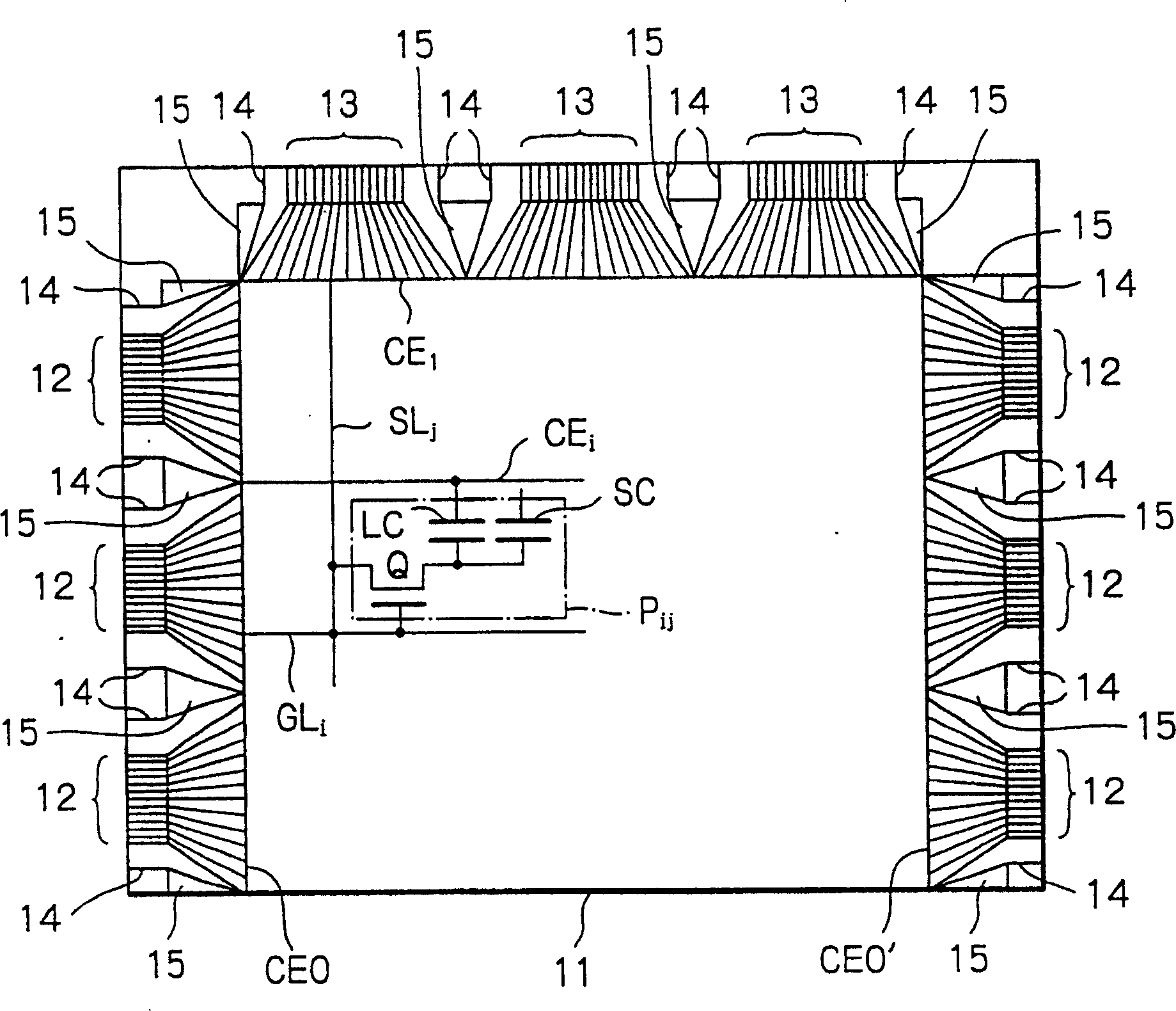
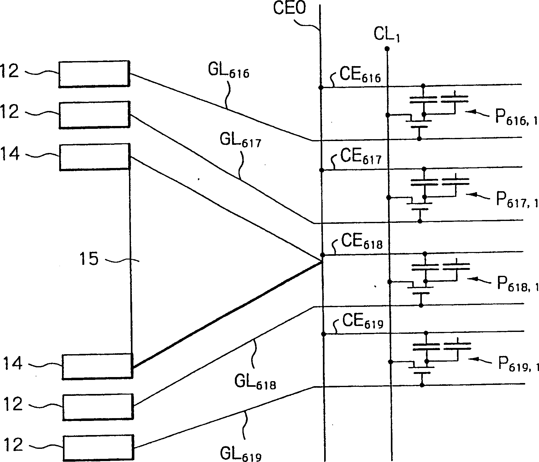
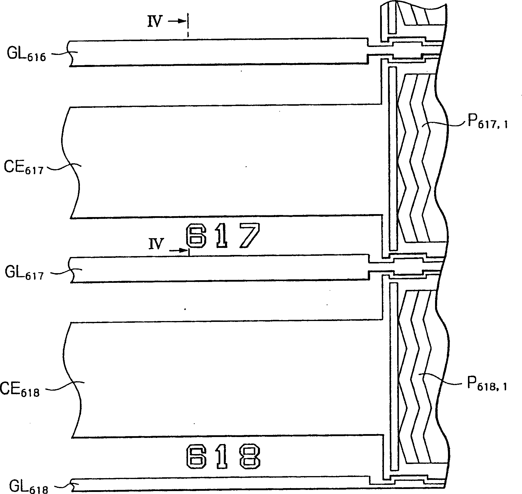
[0021] exist figure 1 In, a plan view of a prior art LCD device is described, and a gate bus line GL is provided on a transparent substrate 11 i (i=1, 2,..., m) and signal bus SL j (j=1, 2,..., n), in the gate bus line GL i and signal bus SL j The intersection of gives a pixel P ij . And the pixel P is formed by a thin film transistor (TFT) Q, a liquid crystal cell LC and a storage capacitor SC ij . In this case, the liquid crystal cell LC is set up with the gate bus GL i A parallel common electrode line CE j connected. Moreover, the storage capacitance SC is connected to an adjacent gate line in the gate storage type or to a storage line (not shown) in the gate storage type, thereby actually increasing the capacitance of the liquid crystal cell LC. .

[0022] In addition, a plurality of gate (scan) lead lines 12 are provided on the transpa...


PUM


Abstract

Including a transparent substrate (11), a plurality of first gate bus lines (GL) formed on the transparent substrate i ), a plurality of second bus lines (SL j ), a plurality of common electrode lines (CE i ), each of a plurality of pixels (P ij ), a plurality of address marks are formed on a transparent substrate, and each address mark is connected to one of the first bus line, the second bus line and the common electrode bus line.

Description

technical field [0001] The present invention relates to liquid crystal display (LCD) devices, and in particular, to an improvement of an address mark for easy and accurate determination of defect locations of LCD devices. Background technique [0002] The LCD devices of the prior art generally include: a transparent substrate, a plurality of gate bus lines formed on the transparent substrate, a plurality of signal bus lines perpendicular to each gate bus line formed on the transparent substrate, A plurality of common electrode lines parallel to each gate bus line are formed, and a plurality of pixels connected to one of the gate bus lines, one of the signal bus lines and one of the common electrode lines. [0003] During the inspection mode, in order to easily and accurately determine defect positions, a plurality of address marks are provided for the gate bus line (common electrode line) and the signal bus line (see JP-A-2000-147549). This will be described in detail below...

Claims


Application Information

Patent Timeline
Patent Type & Authority Patents(China)
IPC IPC(8): G02F1/136G01N21/88G02F1/1343
Inventor 渡边诚志贺俊介
Owner INNOLUX CORP
Features
  • R&D
  • Intellectual Property
  • Life Sciences
  • Materials
  • Tech Scout
  • Unparalleled Data Quality
  • Higher Quality Content
  • 60% Fewer Hallucinations
Learn More