Electrostatic discharge protection on circuit board

A technology for electrostatic discharge protection and circuit boards, which is applied in the direction of static electricity, circuits, and electrical components, and can solve problems such as the failure of the main circuit board 100 to operate normally, processor or chip damage, etc.

Inactive Publication Date: 2006-09-27
LITE ON IT
View PDF0 Cites 0 Cited by
  • Summary
  • Abstract
  • Description
  • Claims
  • Application Information

AI Technical Summary

Problems solved by technology

However, before the electrostatic discharge current flows to the screw 110, the electrostatic discharge current may impact the processor or chip on the main circuit board 100, causing damage to the processor or chip or the main circuit board 100 cannot operate normally.

Method used


Image

  • Electrostatic discharge protection on circuit board
  • Electrostatic discharge protection on circuit board
  • Electrostatic discharge protection on circuit board

Examples


Embodiment Construction

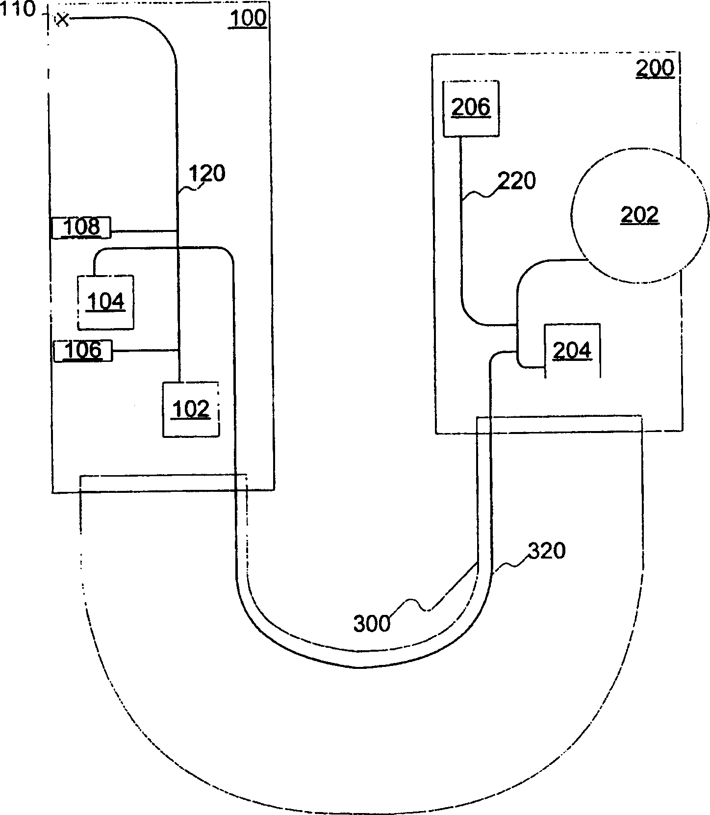
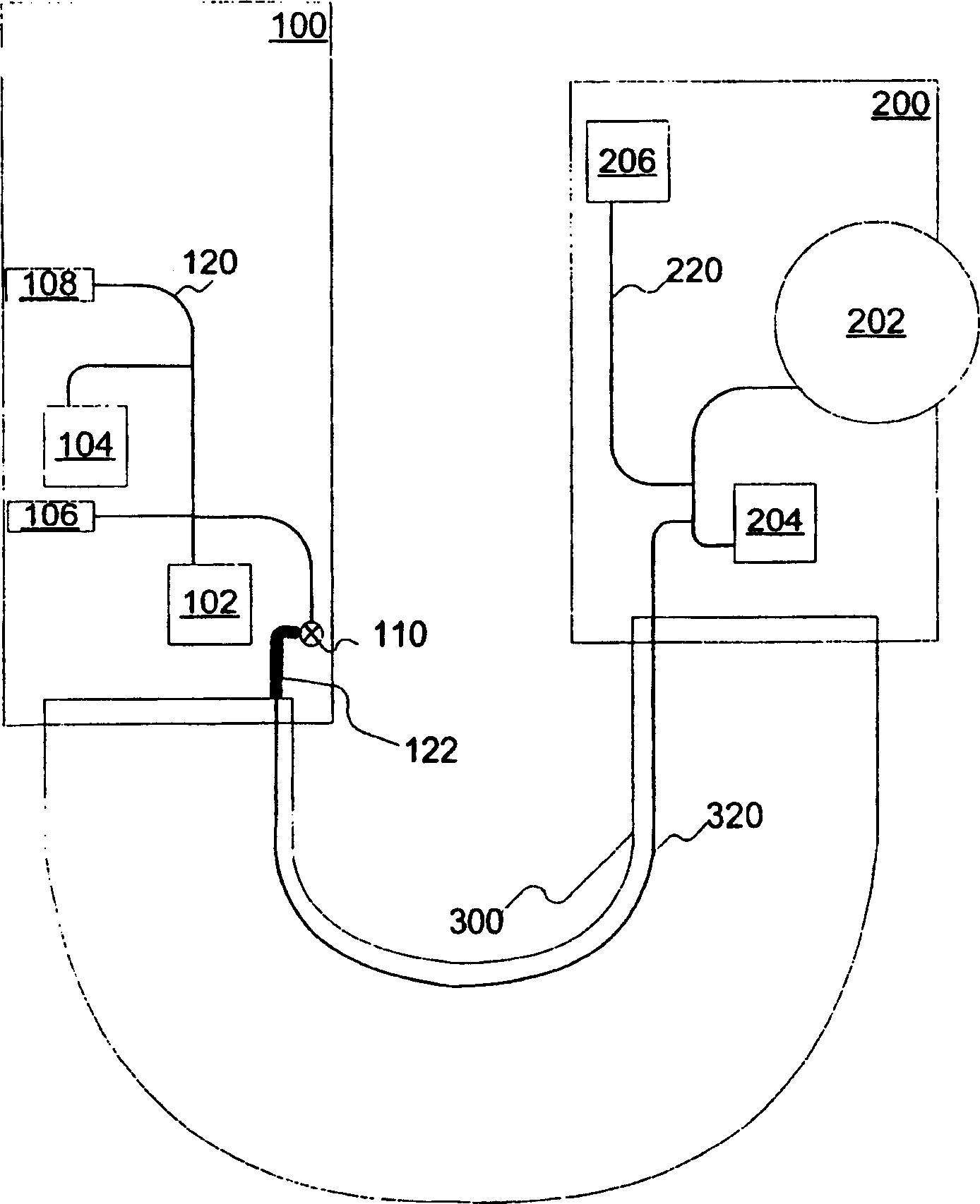
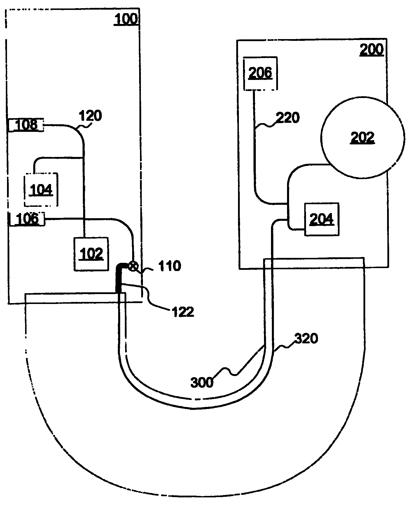
[0020] Please refer to figure 2 , which represents a schematic diagram of circuit board wiring of the thin optical disk device of the present invention. The circuit board of the thin disc device can be divided into two parts, the sub-board (Sub-Board) 200 is fixed on the movable tray (Tray), and the main circuit board (Main Board) 100 is fixed on the casing.

[0021] The present invention first designs an electrostatic discharge protection path 122 on the circuit layout of the main circuit board 100, one end of which is connected to a connection line 320 in the U-shaped flexible cable 300, and the connection line 320 is connected to the ground on the sub-circuit board 200. Line 220 is connected. The other end is directly connected to the screw 110 . According to the embodiment of the present invention, the ESD protection path 122 has a wider line width of 0.75mm, but the above width limit is for reference only, in fact, as long as the line width is greater than the minimum ...


PUM


Abstract

The present invention which is static electrical discharging protection for circuit is applied for two separated circuit boards. It works as that the second circuit board chip is not impacted by static electrical discharging current when static electrical discharging current is generated on the first circuit board so the second circuit board chip is protected from impact of static electrical discharging current.

Description

technical field [0001] This invention relates to electrostatic discharge protection on circuit boards, and more particularly to current protection paths in split circuit boards against electrostatic discharge strikes on other circuit boards. Background technique [0002] Typically, the surface of the human body accumulates an electrostatic charge that can be as large as several thousand volts. If you touch a metal object with your hands, especially a general IC chip or a circuit board embedded with an IC chip, the electrostatic charge on the body will be discharged to the IC chip or circuit board in an instant, which is called Electro Static Discharge (Electro Static Discharge, ESD). The electrostatic discharge current is likely to cause malfunction or damage of the IC chip. [0003] Please refer to figure 1 , which represents a schematic diagram of circuit board wiring of a known thin optical disc device. The circuit board of the thin disc device can be divided into two...

Claims


Application Information

Patent Timeline
Patent Type & Authority Patents(China)
IPC IPC(8): H05F3/02H01L23/60G11B33/14
Inventor 颜加宏赖宏毅高东炜
Owner LITE ON IT
Why Eureka
Try Eureka