Method and apparatus for treating substrate

一种处理方法、处理装置的技术,应用在电气元件、半导体/固态器件制造、电路等方向,能够解决高分子化反应没有充分地进行等问题,达到缩短固化处理时间、消除等待时间、处理时间缩短的效果

Inactive Publication Date: 2006-10-11
TOKYO ELECTRON LTD
View PDF0 Cites 0 Cited by
  • Summary
  • Abstract
  • Description
  • Claims
  • Application Information

AI Technical Summary

Problems solved by technology

[0007] Furthermore, the curing process in the heating furnace is performed in the minimum time for the completion of the polymer reaction in order to increase throughput, so when the film thickness of the interlayer insulating film is thick, it may be high in the deep part of the interlayer insulating film. Molecularization reaction is not fully carried out

Method used


Image

  • Method and apparatus for treating substrate
  • Method and apparatus for treating substrate
  • Method and apparatus for treating substrate

Examples


Embodiment Construction

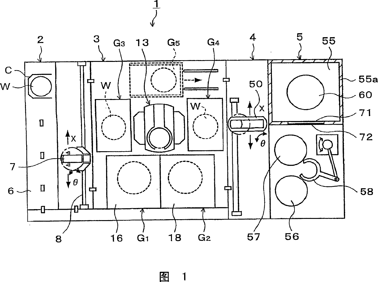
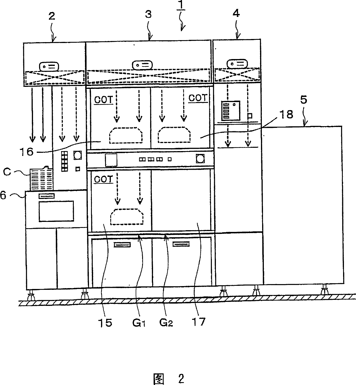
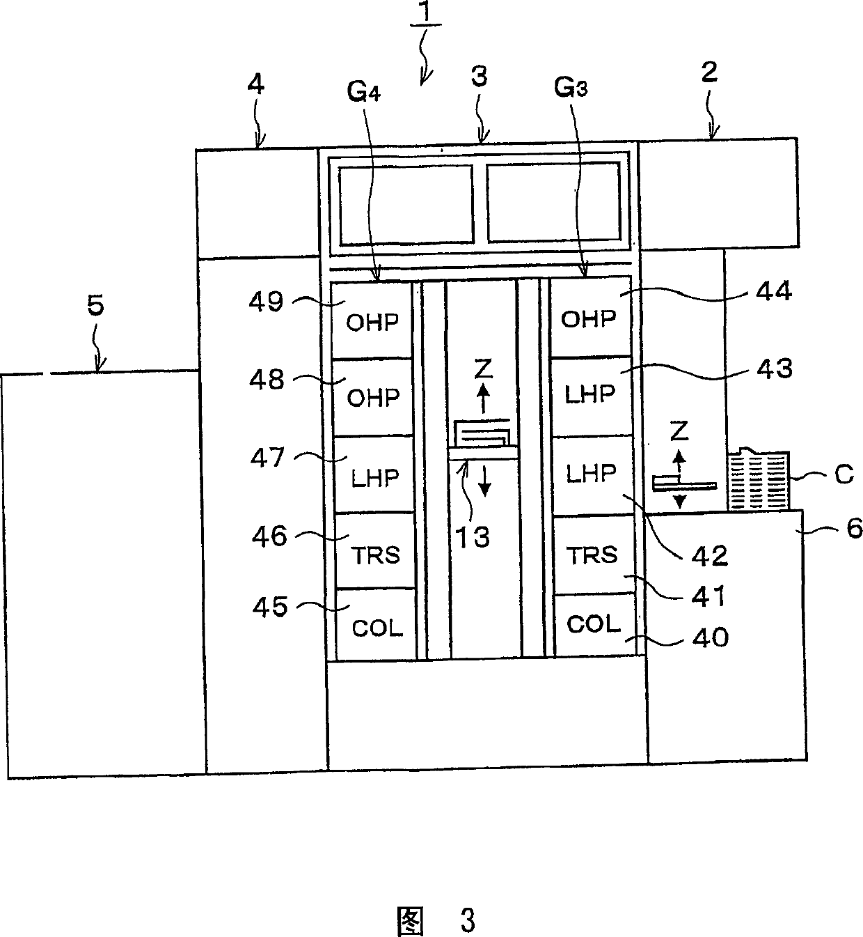
[0044] Next, preferred embodiments of the present invention will be described. 1 is a plan view schematically showing an insulating film forming apparatus 1 for implementing a wafer W processing method according to this embodiment, FIG. 2 is a front view of the insulating film forming apparatus 1 , and FIG. 3 is a rear view of the insulating film forming apparatus 1 .

[0045] As shown in FIG. 1, the insulating film forming apparatus 1 has, for example, a cassette station 2 for loading and unloading wafers W from the outside to the insulating film forming apparatus 1 or loading and unloading wafers W to and from cassette C in cassette units of, for example, 25 wafers W. The first processing station 3 of various processing units that performs predetermined processing individually in the insulating film forming process is provided adjacent to the first processing station 3, and the interface unit 4 that performs delivery of the wafer W, etc., and has a The second processing stat...


PUM


Abstract

The object of the present invention is to form an interlayer insulating film on a substrate, and to cure the interlayer insulating film in a shorter time than the prior art. For this reason, the substrate processing method of the present invention includes: forming an interlayer insulating film on a substrate, irradiating an electron beam to the interlayer insulating film on the substrate in a processing chamber to cure it, and curing the interlayer insulating film after irradiating the electron beam. Finally, plasma is generated in the processing chamber and the potential of the substrate is lowered. Alternatively, the substrate processing method of the present invention includes: forming an interlayer insulating film on the substrate, irradiating the interlayer insulating film on the substrate with electron beams in the processing chamber to cure it, and forming the interlayer insulating film. Cloth becomes the coating process of the coating liquid of interlayer insulating film, and the preheating process of heating substrate is carried out between coating process and interlayer insulating film solidification process, by control device after described preheating process finishes and at The time until the substrate is irradiated with electron beams is controlled to be a certain time. The invention also provides a corresponding substrate processing device.

Description

technical field [0001] The present invention relates to a substrate processing method and a substrate processing device. Background technique [0002] In the manufacturing process of a semiconductor device having a multilayer wiring structure, an interlayer insulating film is formed on a wafer, and then the interlayer insulating film is processed. The so-called interlayer insulating film is an electrically insulating insulating layer in a multilayer wiring structure. As its insulating material, MSQ (methyl silsesquicyclopropane), HSQ (hydrogen silsesquicyclopropane), etc. are used. ). [0003] The processing related to such an interlayer insulating film is carried out in, for example, an SOD (Spin On Dielectric) device in which films are processed by a sol-gel method, a spinning method, a rapid film-forming method, and a focusing method. Forming method, in this film forming method, an interlayer insulating film is formed by applying the aforementioned coating liquid of MSQ...

Claims


Application Information

Patent Timeline
Patent Type & Authority Patents(China)
IPC IPC(8): H01L21/316H01L21/31H01L21/00H01L21/3105H01L21/312
CPCH01L21/02137H01L21/02282H01L21/0234H01L21/02351H01L21/3105H01L21/67109H01L21/67178H01L21/6715H01L21/3124
Inventor 水谷洋二山口正雄
Owner TOKYO ELECTRON LTD
Why Eureka
Try Eureka