

An orthogonal light path type fluorescent detection device for microchip analysis
A fluorescence detection and micro-analysis technology, which is applied in the direction of measuring devices, analysis materials, fluorescence/phosphorescence, etc., can solve the problems of complex optical system structure, difficulty in miniaturization, high price, etc., achieve high detection sensitivity, reduce light scattering, Inexpensive effect
- Summary
- Abstract
- Description
- Claims
- Application Information
AI Technical Summary
Problems solved by technology
Method used
Image

Examples
Embodiment 1
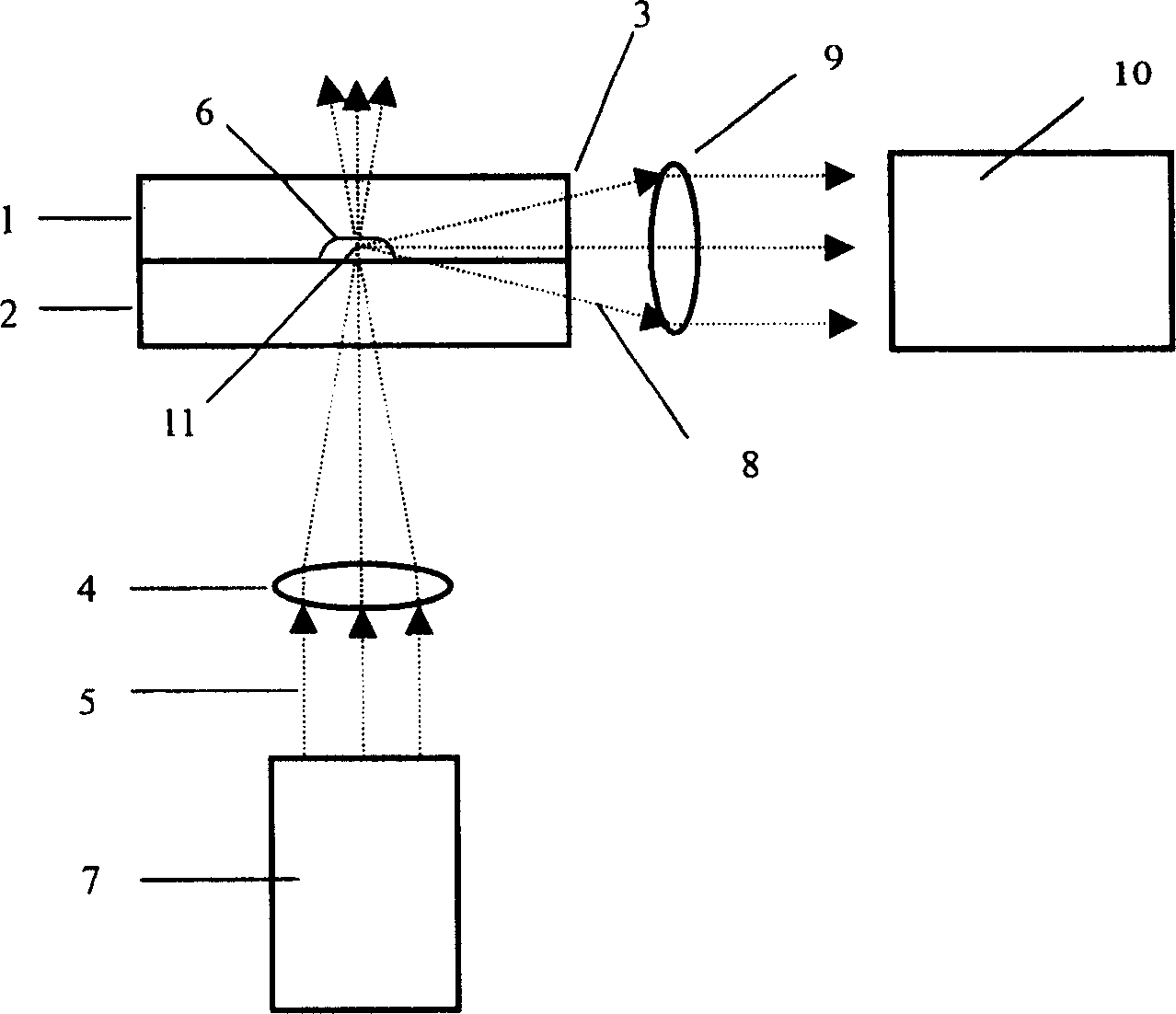
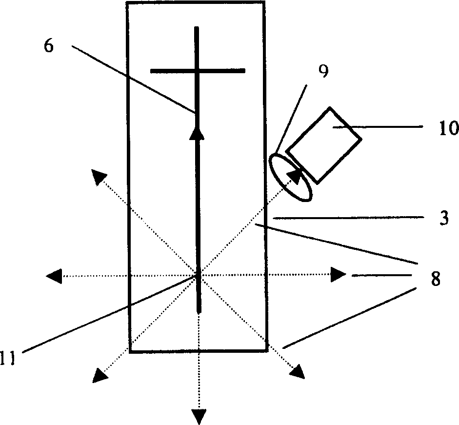
[0024] Refer to attached figure 1 , The microchip is composed of upper 1 and lower 2 glass sheets, and the thickness of the glass sheets is 1.7 mm. A channel is processed on the upper sheet 1 by photomask and wet etching technology, and the width of the microchannel 6 is 60 microns, and the depth is 20 microns. The classic high-temperature bonding method is used to realize the permanent sealing of the upper 1 and lower 2 pieces. A microfluidic chip with a length of 60 mm and a width of 15 mm was obtained. In the present embodiment, the excitation light source 7 is a semiconductor pump laser of 473nm; the excitation light 5 emitted by the laser is focused by the condenser objective lens 4, and enters the chip microchannel 6 from a direction perpendicular to the plane of the lower chip 2 of the chip; 11 emitted, the fluorescence 8 emitted from the chip side wall 3 is collected by the collection objective lens 9 positioned behind the detection window, and the setting direction ...
Embodiment 2
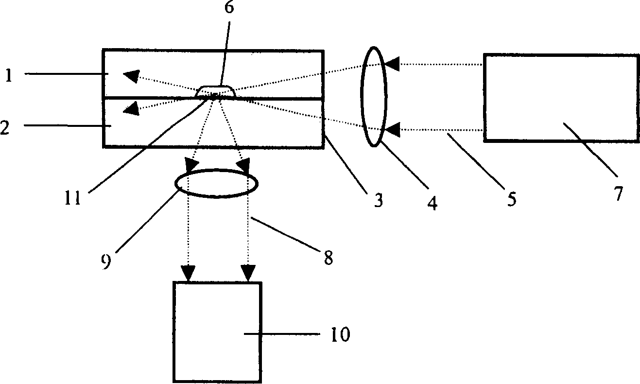
[0027] Refer to attached image 3 After the excitation light 5 emitted by the light source 7 is converged by the focusing objective lens 4, it is incident from the side wall 3 of the chip in a direction perpendicular to the microchannel 6 of the chip; the fluorescent light 8 emitted from the direction perpendicular to the lower chip 2 of the chip is selected, and collected The objective lens 9 collects the stray light, and the stray light is filtered out by the optical filter, and finally the fluorescent signal is detected by the photodetector 10 .
[0028] Figure 4 It is the channel configuration diagram of the micro-analysis chip according to the preferred embodiment 1 of the present invention. The separation channel part of the microchannel 6 on the chip is designed with a bend, near the edge of the side wall 3 of the chip at the end detection area 12, in order to shorten the distance of fluorescence from the light spot to the detection window and improve the collection e...
PUM
| Property | Measurement | Unit |
|---|---|---|
| thickness | aaaaa | aaaaa |
| thickness | aaaaa | aaaaa |
| strength | aaaaa | aaaaa |
Abstract
Description
Claims
Application Information