
Semiconductor memory

A storage device and semiconductor technology, applied in the direction of information storage, static memory, digital memory information, etc., can solve the problems of current consumption, current consumption, and large current consumption of boost power supply circuits, etc.

Inactive Publication Date: 2006-12-20
PANASONIC CORP
View PDF0 Cites 0 Cited by
  • Summary
  • Abstract
  • Description
  • Claims
  • Application Information

AI Technical Summary

Problems solved by technology

[0013] However, as described above, the step-up power supply circuit 113 is always operating in a cycle to generate the Vg voltage, so that unnecessary current is consumed.
The step-up power supply circuit 113 consumes a large current in particular, so there is still the problem of unnecessary current consumption.

Method used


Image

  • Semiconductor memory
  • Semiconductor memory
  • Semiconductor memory

Examples


Embodiment Construction

[0067] Hereinafter, embodiments of the present invention will be described with reference to the drawings.

[0068]

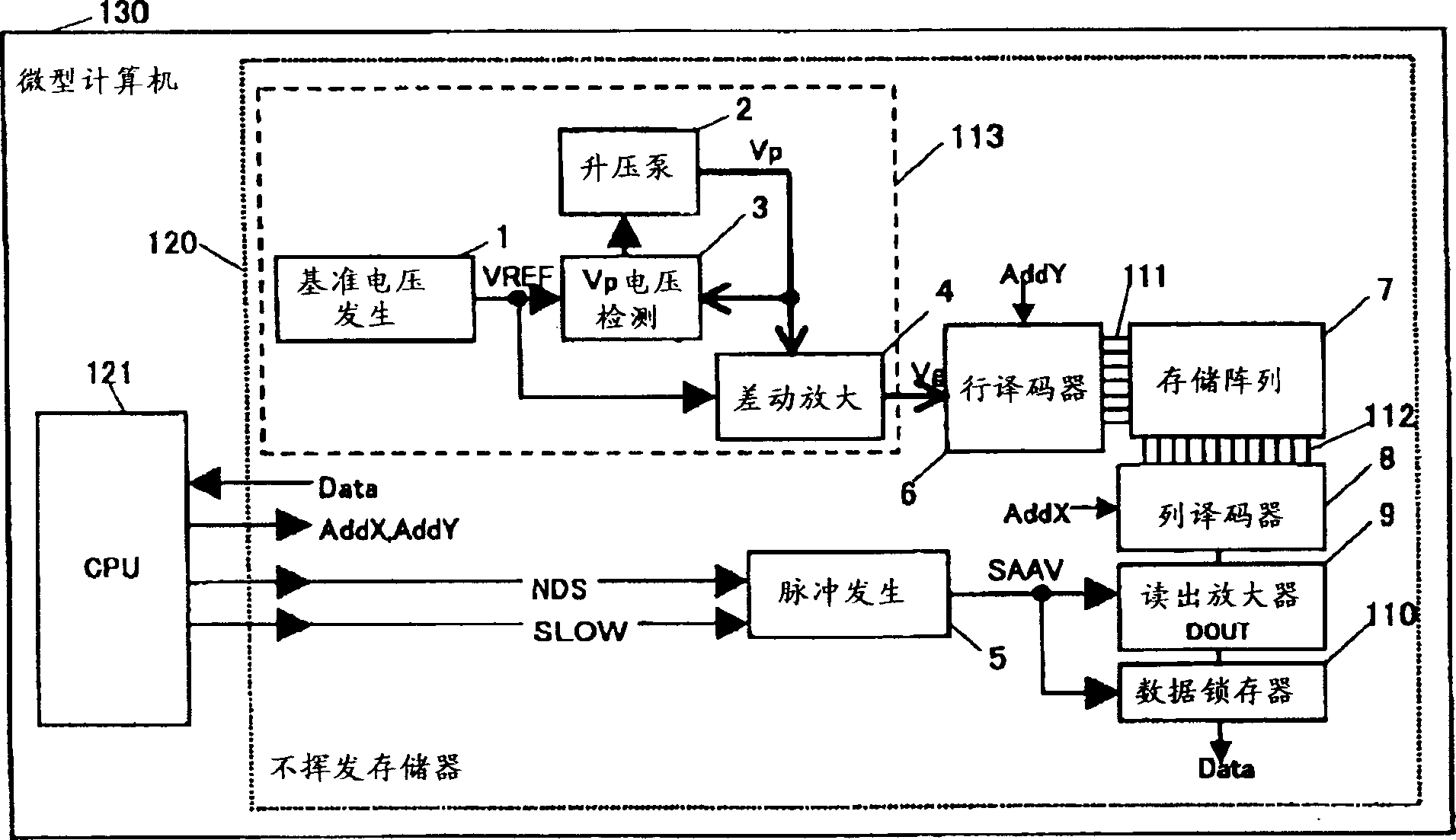
[0069] image 3 The structure of the semiconductor memory device according to the embodiment of the present invention is shown.

[0070] In the same figure, the semiconductor storage device 200 is composed of a step-up power supply circuit 201, a memory cell array 7 in which memory cells storing 1-bit information are arranged in a matrix, and a word line 111 arranged in the Y direction of the memory cell array 7 is passed from Voltage Vg and the address information Add of the CPU to select the row decoder 6 of any word line, wherein the voltage Vg is supplied by the boost power supply circuit 201, and the bit lines 112 arranged along the X direction of the memory cell array 7 are passed through the address from the CPU. Information Add to select the column decoder 8 of any bit line 112, read the sense amplifier 9 of the 1-bit memory cell information selected...


PUM


Abstract

A semiconductor memory device having a memory array is provided. A read unit reads information stored in a memory cell. A step-up unit steps up an externally supplied voltage, and supplies the stepped-up voltage to the memory cell. A start control unit has the step-up unit start the stepping up after a read cycle begins. A detection unit detects that the stepped-up voltage has reached a predetermined level, and has the read unit start the reading upon the detection. A stop control unit has the step-up unit stop the stepping up when a time period required for the reading has elapsed since the detection. With this construction, the time taken for stepping up the voltage supplied to the memory cell is minimized in accordance with the time taken for the reading. Hence the current consumption is reduced when compared with the case where the step-up time is set unnecessarily long.

Description

technical field [0001] The present invention relates to a semiconductor storage device, and in particular to low current consumption technology of a semiconductor storage device having a readout circuit with a built-in boost power supply circuit. Background technique [0002] As one of the readout methods of a semiconductor memory device mounted on a microcomputer device, generally, one of a plurality of memory cells arranged in a matrix is ​​selected by a word line and a bit line, and the selected memory cell is read from the selected memory cell by a sense amplifier. The cell current of the memory cell is used to detect the way information is stored. In addition, in order to supply power to the internal circuit of such a semiconductor memory device, a semiconductor memory device with a built-in step-up power supply circuit for boosting an externally supplied voltage has been developed (for example, Japanese Patent Office, Patent Laid-Open No. 10- Bulletin No. 302492). ...

Claims


Application Information

Patent Timeline
IPC IPC(8): G11C7/00G11C7/24G11C11/34G11C5/14
CPCG11C5/145
Inventor 东亮太郎
Owner PANASONIC CORP
Learn More