

Method for preparing high quality GaN base material on specific saphire pattern substrate
A graphic substrate and sapphire technology, which is applied in semiconductor/solid-state device manufacturing, lasers, electrical components, etc., can solve problems such as low dislocation density, waste of raw materials, and degraded lattice quality, so as to reduce non-radiative recombination centers Corrosion damage, quality improvement effect
- Summary
- Abstract
- Description
- Claims
- Application Information
AI Technical Summary
Problems solved by technology
Method used
Image

Examples
Embodiment 1
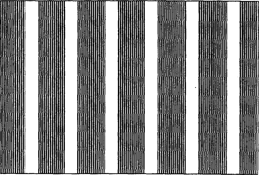
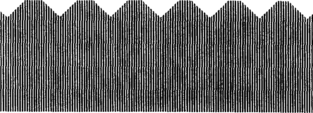
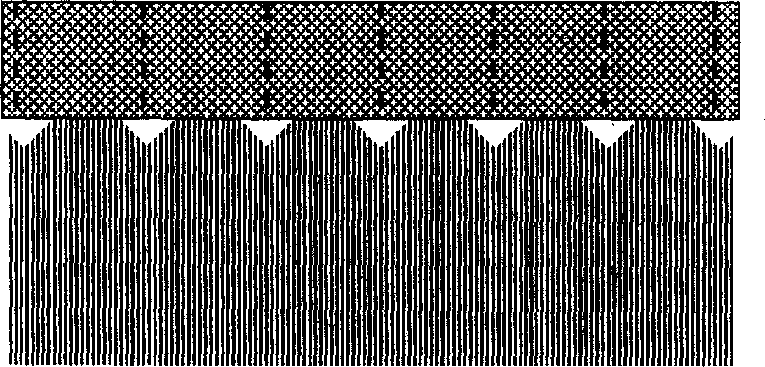
[0025] Using plasma-enhanced chemical vapor deposition (PECVD) to vapor-deposit a silicon dioxide mask layer with a thickness of 200nm on the C-face sapphire; A strip-shaped silicon dioxide mask pattern along the [11 20] direction is etched on the upper surface. The length of the silicon dioxide mask layer stripe pattern is 15mm, the width is 2μm, and the width of the window area is 3μm; put the substrate into In an etching solution mixed with sulfuric acid and phosphoric acid with a volume ratio of 20:1, heat it in a temperature-controlled furnace and etch at 200°C for 1 hour; take out the substrate, rinse it with deionized water, and then put the substrate into In the hydrofluoric acid solution prepared by deionized water and hydrofluoric acid with a volume ratio of 10:1, corrode for 10 seconds; take out the substrate, and rinse it with deionized water for 10 minutes to obtain a clean sapphire pattern substrate. Such as figure 1 , 2 As shown, the mesa of the sapphire patte...
Embodiment 2
[0027]Adopt plasma-enhanced chemical vapor deposition (PECVD) to vapor-deposit a silicon dioxide mask layer with a thickness of 100nm on the C-plane sapphire; A strip-shaped silicon dioxide mask pattern along the [11 20] direction is etched on the upper surface. The length of the silicon dioxide mask layer stripe pattern is 50mm, the width is 4μm, and the width of the window area is 8μm; put the substrate into In an etching solution mixed with sulfuric acid and phosphoric acid with a volume ratio of 10:1, heat it in a temperature-controlled furnace and etch it at 300°C for 2 hours; take out the substrate, rinse it with deionized water, and then put the substrate into In the hydrofluoric acid solution prepared by deionized water and hydrofluoric acid with a volume ratio of 5:1, corrode for 5 seconds; take out the substrate, and rinse it with deionized water for 10 minutes to obtain a clean sapphire pattern substrate. The mesa of the sapphire pattern substrate is periodically ad...
Embodiment 3
[0029] Adopt plasma-enhanced chemical vapor deposition (PECVD) to vapor-deposit a silicon dioxide mask layer with a thickness of 300nm on the C-plane sapphire; A strip-shaped silicon dioxide mask pattern along the [11 20] direction is etched on the upper surface. The length of the silicon dioxide mask layer stripe pattern is 100 mm, the width is 1 μm, and the width of the window area is 10 μm; put the substrate into In an etching solution mixed with sulfuric acid and phosphoric acid with a volume ratio of 5:1, heat it in a temperature-controlled furnace and etch at 400°C for 3 hours; take out the substrate, rinse it with deionized water, and then put the substrate into In the hydrofluoric acid solution prepared by deionized water and hydrofluoric acid with a volume ratio of 20:1, etch for 20 seconds; take out the substrate, and rinse it with deionized water for 10 minutes to obtain a clean sapphire pattern substrate. The mesa of the sapphire pattern substrate is periodically a...
PUM
| Property | Measurement | Unit |
|---|---|---|
| thickness | aaaaa | aaaaa |
| length | aaaaa | aaaaa |
| width | aaaaa | aaaaa |
Abstract
Description
Claims
Application Information