
3D NAND memory and method of forming the same

A 3DNAND, memory technology, applied in semiconductor devices, electric solid state devices, electrical components, etc., can solve problems such as poor contact between the channel layer and the epitaxial silicon layer

Active Publication Date: 2021-05-18
YANGTZE MEMORY TECH CO LTD
View PDF10 Cites 0 Cited by
  • Summary
  • Abstract
  • Description
  • Claims
  • Application Information

AI Technical Summary

Problems solved by technology

[0005] The technical problem to be solved by the present invention is how to prevent the poor contact between the channel layer and the epitaxial silicon layer (SEG)

Method used


Image

  • 3D NAND memory and method of forming the same
  • 3D NAND memory and method of forming the same
  • 3D NAND memory and method of forming the same

Examples


Embodiment Construction

[0034] As mentioned in the background, the existing 3D NAND memory has the problem of poor contact between the channel layer and the epitaxial silicon layer (SEG).

[0035] The study found that the reason for the poor contact between the channel layer and the epitaxial silicon layer (SEG) in the existing 3D NAND memory is that: the existing formation of the epitaxial silicon layer (SEG) is through the selective epitaxial process after the channel hole is formed in the stack structure. However, during the selective epitaxial process, due to the influence of factors such as the depth, size and shape of the channel hole in the stacked structure, the surface of the formed epitaxial silicon layer (SEG) is not flat, and the subsequent formation of the epitaxial silicon layer (SEG) in the channel hole When the charge storage layer and the channel layer are separated, it is easy to cause poor contact between the channel layer and the surface of the epitaxial silicon layer (SEG).

[00...


PUM


Abstract

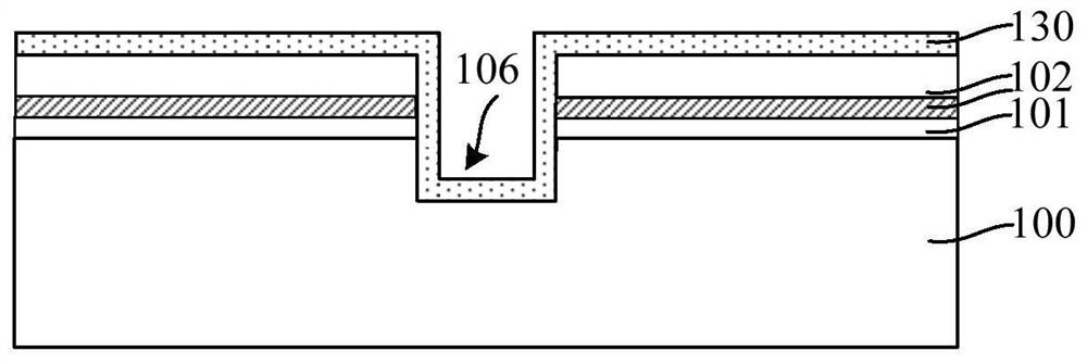
A 3D NAND memory and its forming method, the forming method, before forming the stack structure, a semiconductor epitaxial layer is formed in the groove, when forming the semiconductor epitaxial layer, the forming process will not be affected by the depth of the through hole in the stack structure , size and shape, so that the surface of the formed semiconductor epitaxial layer has a flat surface, so that the channel layer in the storage structure and the semiconductor epitaxial layer can have good contact performance. In addition, the surface of the formed semiconductor epitaxial layer is lower than the surface of the dielectric layer, so that the formed etching stop layer (especially when the etching stop layer is made of metal material) can be limited in the groove above the semiconductor epitaxial layer, so that the etching The stop layer can maintain high position accuracy, and make the dielectric layer have a flat surface, which facilitates subsequent formation of a stacked structure.

Description

technical field [0001] The invention relates to the field of semiconductor manufacturing, in particular to a 3D NAND memory and a forming method thereof. Background technique [0002] NAND flash memory is a better storage device than hard disk drives, and it has been widely used in electronic products as people pursue non-volatile storage products with low power consumption, light weight and high performance. At present, the NAND flash memory with a planar structure is close to the limit of practical expansion. In order to further increase the storage capacity and reduce the storage cost per bit, a 3D NAND memory with a 3D structure is proposed. [0003] The formation process of the existing 3D NAND memory generally includes: forming a stack structure in which silicon nitride layers and silicon oxide layers are alternately stacked on a substrate; etching the stack structure to form channel holes in the stack structure; After the hole, etch the substrate at the bottom of the...

Claims


Application Information

Patent Timeline
Patent Type & Authority Patents(China)
IPC IPC(8): H01L27/115H01L27/11582H01L27/1157H10B69/00H10B43/27H10B43/35
Inventor 李兆松肖莉红刘沙沙卢峰王恩博
Owner YANGTZE MEMORY TECH CO LTD
Learn More