High purity gallium nitride nanometer line preparation method

A gallium nitride nanowire and high-purity technology, which is applied in the field of preparation and generation of inorganic compound semiconductor materials, can solve problems that affect product purity and yield, easily generate by-products, and lengthen the preparation cycle.

Inactive Publication Date: 2007-06-06
TAIYUAN UNIV OF TECH
View PDF4 Cites 2 Cited by
  • Summary
  • Abstract
  • Description
  • Claims
  • Application Information

AI Technical Summary

Problems solved by technology

[0003] In recent years, research on the preparation of inorganic compound gallium nitride nanowires has been mentioned as an important scientific research agenda. The commonly used preparation methods include: sublimation method, catalyst generation method, template method, oxide growth method, laser ablation method, chemical Vapor deposition method, solution reaction method, etc., most of these methods use catalyst or template restriction, which inevitably introduces impurities, which greatly affects the purity and yield of the product, and the raw material ratio of some preparation methods is not enough Strict, unreasonable technological process, resulting in cumbersome preparation methods, prolonging the preparation cycle, and easily generating by-products, making the optical, physical, and chemical properties of the product unstable, affecting the application of the product and the performance of the optoelectronic device. The morphology of the product nanowires changes, the product diameter is unstable, the surface is not smooth enough, and the linear length is not balanced enough

Method used


Image

  • High purity gallium nitride nanometer line preparation method
  • High purity gallium nitride nanometer line preparation method
  • High purity gallium nitride nanometer line preparation method

Examples


Embodiment 1

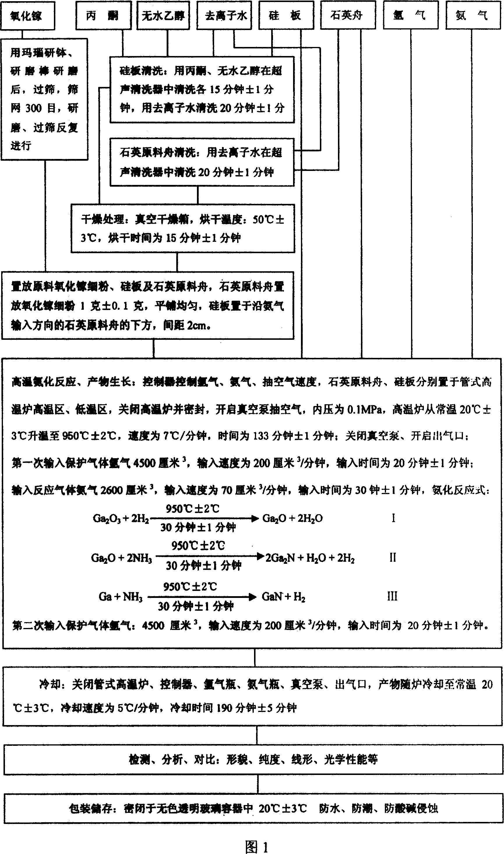
[0107] All preparation equipment is in quasi-working state;

[0108] Accurately weigh according to the ratio, measure 1 g of gallium nitride and 2,600 cm of ammonia 3 , Argon 9000 cm 3 , 20ml acetone, 20ml absolute ethanol, 140ml deionized water;

[0109] Grinding and sieving: The gallium oxide is repeatedly ground and sieved to form a fine powder with a 300 mesh screen;

[0110] Ultrasonic cleaning of silicon plates: 20 ml of acetone, 20 ml of absolute ethanol, 40 ml of deionized water;

[0111] Ultrasonic cleaning quartz raw material boat: 100ml deionized water;

[0112] Drying treatment: the silicon plate and quartz raw material boat are dried in a drying box at a temperature of 50℃±3℃;

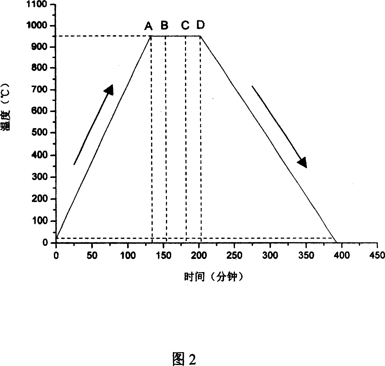
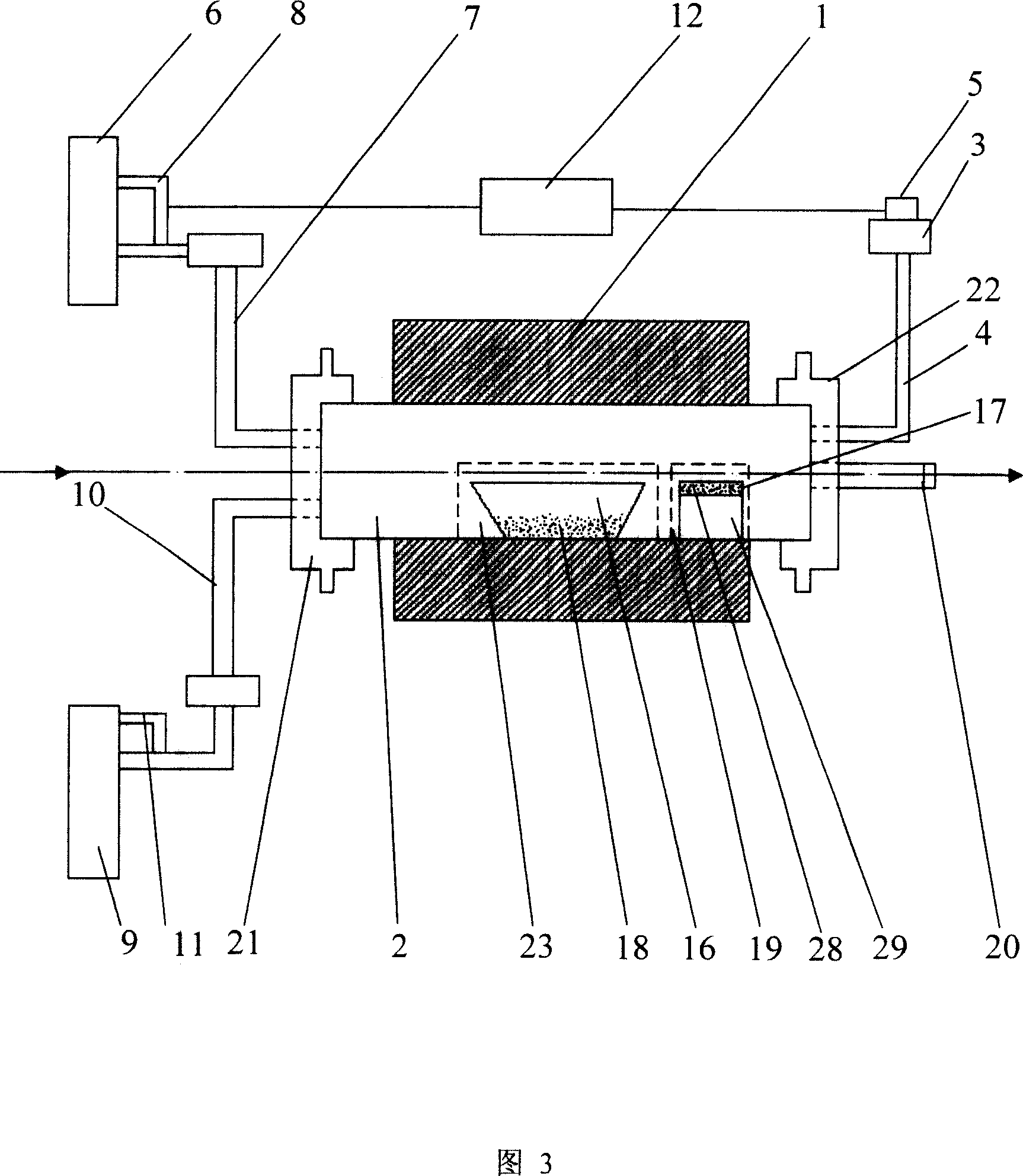
[0113] Place raw materials, silicon plates, and quartz raw materials boat: the fine gallium oxide powder is placed in the quartz raw material boat, the quartz raw material boat is placed in the high temperature zone of the tubular high temperature furnace, and the silicon plate is placed in th...


PUM

PropertyMeasurementUnit
lengthaaaaaaaaaa

Abstract

The invention discloses a process for preparing a kind of gallium nitride nanoline of high purity, which employs gallium oxide (Ga2O3) as raw material, alkaline air (NH3) as reacting gas, inert gas argon gas (Ar) as protective gas, silicon board as base carrier for product growing, absolute ethyl alcohol, acetone and deionized water as cleaning agent for the sicicon board, and employs no accelerating agent; the gallium nitride nanoline grows out under the temperature of 950 Deg C and on the silicon board through ammonification reaction; the preparing process is simplified by grinding, sifting the raw material, cleaning the silicon board and quartz material, controlling the air extraction, argon gas and alkaline air inputting by tubing high temperature furnace control device procedurally, which prevents the side product generating effectively and increases the product outcome, purity and quality and finally getting the gallium nitride nanoline of light yellow, solid and in linary shape; the product is characterized by the uniform shape, order arrangement, and stable optical, chemical and physical property; the invention is characterized by the short preparing process, high yield (reaching to 95%), high purity (reaching to 98.6%) and the high linary accuracy, with the diameter being 5-20 cm, the average length of the monoline 30-50 mum.

Description

Technical field [0001] The invention is a method for preparing high-purity gallium nitride nanowires, and belongs to the technical field of methods for preparing and generating inorganic compound semiconductor materials. Background technique [0002] Semiconductor nanowires and carbon nanotubes are the raw materials for manufacturing nanoscale electronic and optical devices. Gallium nitride nanowires of one-dimensional III-V compounds have unique optical and electrical properties. They are used in visible light, ultraviolet light and other optoelectronic devices. It has broad application prospects. It is a wide direct band gap semiconductor with high electron saturation drift speed. It is one of the most superior materials for manufacturing blue light diodes and high-power optoelectronic devices. [0003] In recent years, the preparation of inorganic compound gallium nitride nanowires has been mentioned in the important scientific research agenda. The commonly used preparation me...

Claims


Application Information

Patent Timeline
Patent Type & Authority Patents(China)
IPC IPC(8): C01B21/06C01G15/00F27B3/04
Inventor 许并社翟雷应梁建贾虎生刘旭光郝海涛李春华
Owner TAIYUAN UNIV OF TECH
Why Eureka
Try Eureka