Method and apparatus for controlling the common mode impedance misbalance of an isolated sigle-ended circuit

A common-mode impedance and circuit technology, applied in the direction of amplifier input/output impedance improvement, amplifiers with semiconductor devices/discharge tubes, electrical components, etc., can solve common-mode current reduction, common-mode current imbalance, and common-mode impedance increase And other issues

Inactive Publication Date: 2002-05-15
MEDTRONIC PHYSIO CONTROL MFG
0 Cites 4 Cited by

AI-Extracted Technical Summary

Problems solved by technology

The proximity of the ground plane of the device to ground creates parasitic capacitance (represented by capacitor 28) and reduces common-mode current due to increased common-mode impedance
However, as in Figure 1A, t...

Abstract

A method and apparatus for controlling the common mode impedance misbalance of an isolated single-ended circuit for all common mode paths, thereby allowing the balancing of the common mode impedances which reduces common mode effects while maintaining the advantages of the single-ended amplifier including circuit simplicity and the reference input connected to circuit ground.

Application Domain

Differential amplifiersAmplifier input/output impedence modification +1

Technology Topic

Electronic circuitCapacitor +3

Image

  • Method and apparatus for controlling the common mode impedance misbalance of an isolated sigle-ended circuit
  • Method and apparatus for controlling the common mode impedance misbalance of an isolated sigle-ended circuit
  • Method and apparatus for controlling the common mode impedance misbalance of an isolated sigle-ended circuit

Examples

  • Experimental program(1)

Example Embodiment

[0044] The present invention requires that the shielded circuit be isolated from the ground ground. Two implementations can be taken: isolate the entire device including the shielded circuit; or use an isolation barrier between the circuit that is not isolated from the ground and the shielded circuit. The second embodiment requires isolated power and data transmission circuits. The present invention can adopt any embodiment.
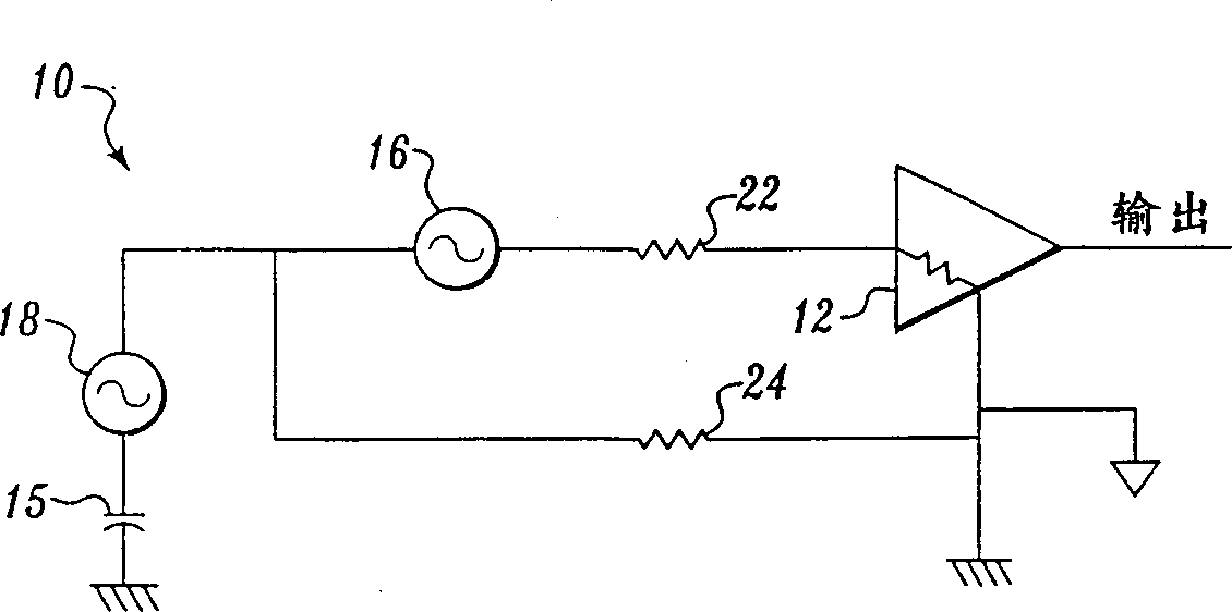
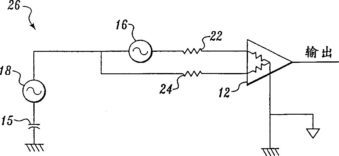
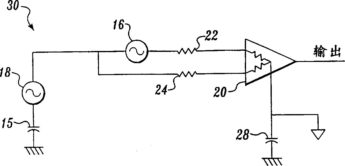
[0045] Figure 2A with 2B The working principle of the described embodiment is to match the discrete capacitor with the parasitic capacitance formed between the shield and the ground layer or with the internal shield. in Figure 2A In the schematic diagram 34, a physical “outer” shield 42 enclosing an “inner” physical shield 46A is provided, and the “inner” physical shield 46A itself encloses the amplifier 26. One end of the noise source 18 is coupled to a capacitor 15 representing the parasitic capacitance between the ground ground and the noise source. The other end of the noise source 18 is coupled in parallel at terminal A to one end of a resistive wire (represented by resistor 22) and one end of another resistive wire (represented by resistor 24). The other end of resistor 22 is coupled to the input of amplifier 26, and the other end of resistor 24 is coupled to the reference of amplifier 26, which is also circuit grounded. In addition, a small signal source (not shown) inserted between the resistors 22 and 24 provides a small signal for amplification.
[0046] The physical outer shield 42 made of conductive material encloses the physical inner shield 46A and the amplifier 26. The capacitor 36A is coupled between the physical inner shield 46A and the physical outer shield 42 and represents the parasitic capacitance between the inner shield and the outer shield. The capacitor 38A is coupled between the physical outer shield 42 and the ground ground and represents the parasitic capacitance between the physical outer shield and the ground ground. The discrete capacitor 40A is connected between the physical outer shield 42 (at terminal B) and the input of the amplifier 26 (terminal C). The value of the capacitor 40A (Farads) is selected to match the parasitic capacitance formed by the proximity of the inner shield 46A and the outer shield 42. This parasitic capacitance is represented by the capacitor 36A so that a common mode signal appears in all inputs of the amplifier 26 (including the reference input) The balanced impedance. In this manner, the present invention provides a relatively balanced impedance between the input of amplifier 26 and any common mode current loops. Also, the value of the capacitor 40A is rated as the maximum voltage applied to the circuit under all conditions, for example, switching high-voltage circuits that cost the inventive circuit requires the capacitor 40A to be rated as high as 5000 volts. Although not shown, it should be understood that the amplifier circuit 26 in the inner shield 46A can be replaced by other electronic circuits. For example, an A/D converter can be used in the present invention to reduce the influence of external noise sources on the sampled input signal.
[0047] Although not shown, it is foreseen that a matching resistor can be coupled between the outer shield 42 and the inner shield 46A instead of using the matching capacitor 40A to compensate for the unbalanced parasitic capacitance. In another embodiment, a matching resistor (not shown) may be connected in series with the matching capacitor 40A between the outer shield 42 and the inner shield 46A. In this case, if the matching capacitor 40A is not in the closed position, the matching resistor will continue to balance the impedance of the common mode signal although the performance achieved by the matching resistor is reduced compared with the matching capacitor.
[0048] It is foreseen that the present invention can use high voltage circuits such as defibrillator circuits. The optional defibrillator shown in dashed lines is enclosed in a physical inner shield 46A and includes a high voltage discharge capacitor 37 coupled between circuit ground and inductance 39. The switch 41 shown in dashed lines is used to optionally connect the capacitor 37 and the inductor 39 with the input connected to the resistor 22 for the purpose of defibrillation. In this way, the amplifier 26 can sense small signals such as the electrocardiogram signal of the terminal A until it decides to deliver the waveform from the defibrillation circuit to the patient via the resistive wires (resistors 22 and 24). Resistors 22 and 24 represent the source resistance present in the patient, and therefore are the partial resistance of the patient or at least the combined resistance of the patient and a pair of electrodes coupled to the patient via a resistive wire.
[0049] Optionally, the surge protector 45 (shown in dashed line) and the resistor 44 (shown in dashed line) or the surge protector 45 are separately coupled in series between the outer shield 42 and the inner shield 46A, and act as a shield Connect to the circuit ground when it cannot be electrically isolated from the level existing in the circuit. The surge protector 45 and the resistor 44 have no effect on the CMRR or any capacitance in the circuit. On the contrary, they only work in the circuit when there is a surge voltage. For example, when the present invention is used in a device such as a defibrillator, the shield can be loaded with a high voltage of up to 5000 volts or higher. The use of the surge protector 45 and the resistor 44 can clamp the voltage on the shield to the order of 100 volts during the delivery process of the defibrillator. The value (ohms) of resistor 44 is selected to limit the amount of inrush current flowing through the surge protector. In one embodiment, the surge protector 45 may be an "air gap" device, which is rated for a maximum voltage of 90 volts, and the value of the resistor 44 may be 4000 ohms. In this embodiment, the physical outer shield 42 only needs to be configured to withstand a maximum voltage slightly greater than the rating of the surge protector 45, such as 90 volts, instead of the high voltage circuit with a voltage rating of up to 5000 volts. In addition, although not shown in the drawings discussed below, the resistor 44 and the surge protector 45 may also be coupled in series between the circuit ground and the shield (physical or grid type) placed in any of the configurations described below.
[0050] In another embodiment, another connection can be established between the physical outer shield 42 and the terminal A through a series resistor 23 (indicated by a dashed line). This connection provides a lower impedance path for common mode noise currents because this current does not have to flow through capacitors 36A and 40A. This effectively shunts the common mode noise current from the resistors 22 and 24, thereby generating a smaller voltage drop across these resistors and thus reducing the possibility of common mode to differential mode conversion.
[0051] In addition, for example, by using a shielded cable, the connection medium between the signal source and the electronic circuit can be shielded. In this case, the shield of each cable from the signal source should be connected to the outer shield.
[0052] Look now Figure 2B , Overview 48 shows that the closure is basically the same as Figure 2A The circuit shown is a physical shield for a comparable amplifier circuit. The difference is that in this case, the internal physical shield 46B is conceived as a ground plane, and thus does not completely enclose the amplifier 26. The discrete capacitor 40B is coupled between the outer shield 42 and the non-reference input of the amplifier 26. The value (Farads) of the capacitor 40B is selected to match the parasitic capacitance formed by the proximity of the inner shield 46B and the outer shield 42. This parasitic capacitance is represented by the capacitor 36B, so that the common mode appears in all inputs of the amplifier 26 (including the reference input). The balanced impedance of the signal. In this manner, the present invention provides a relatively balanced impedance between the input of amplifier 26 and any common mode current loops.
[0053] image 3 Describing the discrete components and parasitic capacitances in the amplifier circuit 66, the circuit 66 uses a non-physical or grid-type shield used with an electronic circuit such as a defibrillator. Common mode noise can be introduced into the loop at any point; the two common mode sources come from the operator and/or patient connected to the electronic circuit. One end of the operator noise source 72 is coupled to the ground through a parasitic capacitance 74, and the other end of the operator noise source is coupled in parallel to one end of the capacitor 68 (operator-shield parasitic capacitance) and the capacitor 70 (operator-circuit ground) Parasitic capacitance). The other end of capacitor 68 is coupled to the non-physical shield at terminal E, and the other end of capacitor 70 is coupled to circuit ground at terminal F. The connections between the operator noise source 72, the capacitor 68, the capacitor 70, the non-physical shield and the circuit ground are drawn with dashed lines, indicating that these components are only present when the operator uses (nears or touches) the components related to the circuit .
[0054] One end of the capacitor 38 (the parasitic capacitance between the shield and the ground ground) is coupled to the ground ground and the other end is coupled to the non-physical shield at the terminal E. One end of the capacitor 36 (the parasitic capacitance between the shield and the circuit ground layer) is coupled to the terminal E (non-physical shield) and the other end is coupled to the circuit ground at the terminal F. One end of the discrete (shield-amplifier) ​​capacitor 41 is coupled to the end point E (shield) and the other end is coupled to the non-reference input of the amplifier 20 and one end of the resistor 22. The other end of the resistor 22 is coupled to one end of the resistor 24 and one end of the patient noise source 76. The other end of the resistor 24 is coupled to the circuit ground at the terminal F. Also, the other end of the patient noise source 76 is coupled to one end of the capacitor 78 (patient-ground parasitic capacitance). The other end of the capacitor 78 is coupled to ground.
[0055] In addition, one end of the capacitor 64 (the parasitic capacitance between the circuit ground layer and the ground ground) is coupled to the terminal F (circuit ground) and the other end is coupled to the ground ground.
[0056] For the above-mentioned defibrillator, the use of non-physical shielding causes several considerations that are different from the use of physical (complete) shielding. By ignoring the influence of the operator (operator noise source 72 and capacitors 68, 70, and 74), the current flowing from patient noise source 76 through resistors 22 and 24 must be balanced for these two resistors. This means that the impedance from the patient noise source 76 to ground at the other end of the resistors 22 and 24 must be the same. In order to balance this impedance without using discrete capacitor 41, the value of capacitor 38 (parasitic capacitance between shield and ground) must be equal to the value of capacitor 64 (parasitic capacitance between circuit ground and ground). In situations where it is difficult to match the capacitors 38 and 64, a discrete capacitor 41 connected in series with the capacitor 38 can be added so that the series combination of the capacitors 38 and 41 is equal to the value of the capacitor 64.
[0057] Second, when considering the influence of the operator (operator noise source 72 and capacitors 68 and 79), the ratio of the value of capacitor 68 to the value of capacitor 38 must be equal to the ratio of the value of capacitor 70 to the value of capacitor 64. By making these ratios equal, the voltage generated by the operator noise source 72 at the amplifier input will be the same. Since the value of the discrete shield-amplifier capacitor 41 is chosen to be larger than that of the other parasitic capacitors, there is a relatively small voltage drop across the discrete capacitor 41, and the balance of these ratios results in a relatively small voltage drop at the input of the amplifier 20. Balanced voltage. There are two voltage dividers, one on each side of the "H-bridge" circuit, and the impedance in each branch does not have to be equal. Make the ratio from top to bottom equal to balance the bridge. Moreover, since the parasitic capacitance between the shield and the circuit ground (capacitor 36) is not very large in the non-physical shield embodiment, the discrete shield-amplifier capacitor 41 is not selected to match the value of the capacitor 36.
[0058] Figure 4A with 4B Shows that it works differently than Figure 2A with 2B The grid-type shielding embodiment of the embodiment. in Figure 4A In, the schematic diagram 50 shows a grid-type "outer" shield 54 that encloses an "inner" physical shield 58A, which in turn encloses the amplifier 20. One end of the noise source 18 is coupled by a capacitor 15 (parasitic capacitance between the noise source and the ground). The other end of the noise source is coupled in parallel to one end of a resistive wire (represented by resistor 22) and one end of another resistive wire (represented by resistor 24) at terminal A. The other end of resistor 22 is coupled to the non-reference input of amplifier 20 and the other end of resistor 24 is coupled to circuit ground which is also the reference input of the amplifier. In addition, the small signal source 16 is coupled in series between the ends of the resistors 22 and 24 at the terminal A (not shown), and this signal source provides a small signal for amplification.
[0059] The grid type shield 54 made of conductive material encloses the solid inner shield 58A, and the shield 58A itself encloses the amplifier 20. The capacitor 36C (outer grid shield-physical inner shield parasitic capacitance) is coupled between the physical inner shield 58A and the outer grid shield 54. The capacitor 38B (the parasitic capacitance between the grid shield and the ground ground) is coupled between the grid shield and the ground ground. Furthermore, the capacitor 52A (the parasitic capacitance between the physical internal shield and the ground ground) is coupled between the physical internal shield and the ground ground.
[0060] The discrete capacitor 41A is connected between the grid shield 54 and the non-reference input of the amplifier 20. Select and locate the grid shield, such as image 3 The total capacitance ratio is balanced as described. Thus, a relatively balanced impedance is formed between the input of the amplifier and any common-mode current loop.
[0061] The fineness of the intervals in the grid shield 54 is preferably selected to be smaller than the relative "touch points" of the noise source of the applied electric field, such as the user's fingers. In this way, the parasitic capacitance generated by the approach of the finger with respect to the grid shield is balanced by the parasitic capacitance generated between the finger and the amplifying circuit element including the circuit ground layer. The size of the intervals of the grid shield is set so that the electric field surrounding the finger acts on the multiple intervals of the grid shield.
[0062] Moreover, the thickness of the wire forming the grid shield 54 is preferably selected so that the amplifying circuit element is "recognized" by the electric field surrounding the user's finger. For example, a grid-type shield that is arranged far from the amplifying circuit may use a thinner wire than a grid-type shield that is close to the circuit. In this way, the larger "holes" created by the thinner wires in the grid shield will reduce the imbalance in the parasitic capacitance generated between the finger and the external grid and between the finger and the amplifying circuit element. Moreover, the thickness of the grid shield can be selected to accommodate the positioning of the battery, as long as the total capacitance ratio remains balanced.
[0063] in Figure 4B In, overview 56 shows a pair of closed basically and Figure 4A The shown circuit is comparable to the shielding of the amplifying circuit. The difference is that in this case, the internal physical shield 58 can be conceived as a ground plane, and thus does not completely enclose the amplifier 26. The discrete capacitor 41A is coupled between the grid shield 54 and the non-reference input of the amplifier 20. The grid shield is selected and positioned so that the total capacitance ratio is balanced as described above. Thus, a relatively balanced impedance is formed between the input of the amplifier and any common-mode current loop.
[0064] Figure 5A-5E It is shown that the present invention uses different configurations of high-voltage defibrillation devices. in Figure 5A In the figure, a side cross-sectional view of the defibrillator 100A is shown, and the defibrillator 100A includes a housing 112 generally made of a non-conductive material. The circuit board 104 is placed in the housing 112. The controller 110, a pair of electrodes 102A and 102B, a power source 106 and a discharge capacitor 108 are coupled to the circuit board 104. The "outer" shield 134 encloses the outside of the housing 112 of the defibrillator 100A and the components placed in the housing, namely the circuit board 104, the power supply 106, and the capacitor 108. The capacitive element 136 is formed by placing a conductive plate on the inside of the housing 112 and couples it to the non-reference input of the amplifying circuit on the circuit board 104. The location and size of the capacitive element are selected to match the parasitic capacitance between the physical outer shield and the physical inner shield or optionally between the circuit ground plane.
[0065] in Figure 5B Here, a side cross-sectional view of the defibrillator 100B is shown, and the defibrillator 100B includes a housing 112 generally made of a non-conductive material. The circuit board 104 is placed in the housing 112. The controller 110, a pair of electrodes 102A and 102B, a power source 106 and a discharge capacitor 108 are coupled to the circuit board 104. The capacitor 109B is coupled between the shield 114 and the non-reference input of the amplifying circuit on the circuit board 104. For the physical shield, the size of the capacitor 109B is selected to match the parasitic capacitance between the physical shield and the circuit ground plane. However, for non-physical shielding, the value of capacitor 109B is chosen to be significantly larger than the parasitic capacitor in the circuit. Optionally, a surge protector 45 and a resistor 44 (shown in dashed lines) may be connected between the shield 114 and the circuit ground to provide substantially the same function as described above. Moreover, a wire 116 (shown in dashed lines) may be coupled between the open ends of the U-shaped conductive shield 114.
[0066] Figure 5C To show a side cross-sectional view of the defibrillator 100C, the defibrillator 100C is basically the same as Figure 5B The difference is that two substantially flat conductive shields are arranged on the top or bottom of the housing 112, respectively. The top shield 118 is placed between the housing 112 and the top of the circuit board 104. The bottom shield 120 is placed between the housing 112 and the power source 106, the discharge capacitor 108, and the bottom of the circuit board 104. At least one of the wires 122 and 124 is coupled between similarly arranged ends of the top shield 118 and the bottom shield 120. Moreover, the capacitor 109C is coupled between the shield 118 and the non-reference input of the amplifier circuit on the circuit board 104. For the physical shield, the size of the capacitor 109C is selected to match the parasitic capacitance between the shield and the circuit ground plane. However, for non-physical shielding, the value of capacitor 109C is chosen to be significantly larger than the parasitic capacitor in the circuit.
[0067] Figure 5D To show a side cross-sectional view of the defibrillator 100D, the defibrillator 100D is basically the same as Figure 5B The difference is that the conductive shield 126 with a substantially planar surface is formed in a U-shape, and the U-shaped shield encloses the circuit board 104 and the discharge capacitor 108 but does not enclose the bottom of the power supply 106. The wire 128 is optionally connected between the open ends of the U-shaped conductive shield 126. Moreover, the capacitor 109D is coupled between the shield 126 and the non-reference input of the amplifier circuit on the circuit board 104. In this embodiment, the conductive shield 126 may be a non-physical (grid-type) shield, and the shield is selected and positioned to be compatible with image 3 with 4A Work in the manner described in /B. For non-physical shielding, the value of capacitor 109D is chosen to be significantly larger than the parasitic capacitor in the circuit.
[0068] Figure 5E To show that it is basically the same as Figure 5B A side cross-sectional view of a similar defibrillator 100E. The internal conductive shield 132 encloses the circuit board 104. The outer conductive shield 130 encloses the power supply 106, the discharge capacitor 108, and the inner shield 132 that houses the circuit board 104. Moreover, the capacitor 109E is coupled between the external shield 134 and the non-reference input of the amplifier circuit on the circuit board 104. When the outer shield 130 is a physical shield, the size of the capacitor 109E is selected to match the parasitic capacitance between the physical outer shield 130 and the circuit ground layer. However, when the external shield 130 is a non-physical (grid-type) shield, the value of the capacitor 109E is selected to be significantly larger than the parasitic capacitor in the circuit. Moreover, the non-physical shield 130 is selected and located and works in the manner described above.
[0069] An important aspect of the present invention is that the common mode noise of the single-ended input of the amplifier is truly eliminated by balancing the parasitic capacitance with a matched capacitor and at least one conductive shield. Although some of the above-mentioned embodiments of the present invention use amplifier circuits for defibrillators, it is foreseen that the present invention can also use any type of electronic devices that amplify small signals, such as electronic meters for measuring small signals and in telecommunications and audio amplifiers. Electronic equipment in industry. It is also foreseeable that the present invention can improve the existing amplifying circuit to provide higher CMRR.

PUM

no PUM

Description & Claims & Application Information

We can also present the details of the Description, Claims and Application information to help users get a comprehensive understanding of the technical details of the patent, such as background art, summary of invention, brief description of drawings, description of embodiments, and other original content. On the other hand, users can also determine the specific scope of protection of the technology through the list of claims; as well as understand the changes in the life cycle of the technology with the presentation of the patent timeline. Login to view more.
Why Eureka
Try Eureka