
Charge pump circuit, integrated circuit, electronic device and method therefor

Active Publication Date: 2016-05-05
MEDIATEK SINGAPORE PTE LTD SINGAPORE
View PDF3 Cites 4 Cited by
  • Summary
  • Abstract
  • Description
  • Claims
  • Application Information

AI Technical Summary

Benefits of technology

The patent text describes a method to reduce the time it takes to start up a negative voltage generation circuit for a charge pump. This is accomplished by providing a maximum charging supply voltage to the charge pump circuit and using a two-phase clock generator to provide non-overlapping clock signals with different voltage levels. This prevents low impedance paths that could impact the efficiency of the charge pump.

Problems solved by technology

However, such known negative voltage generation circuits suffer from one or more of the following problems.
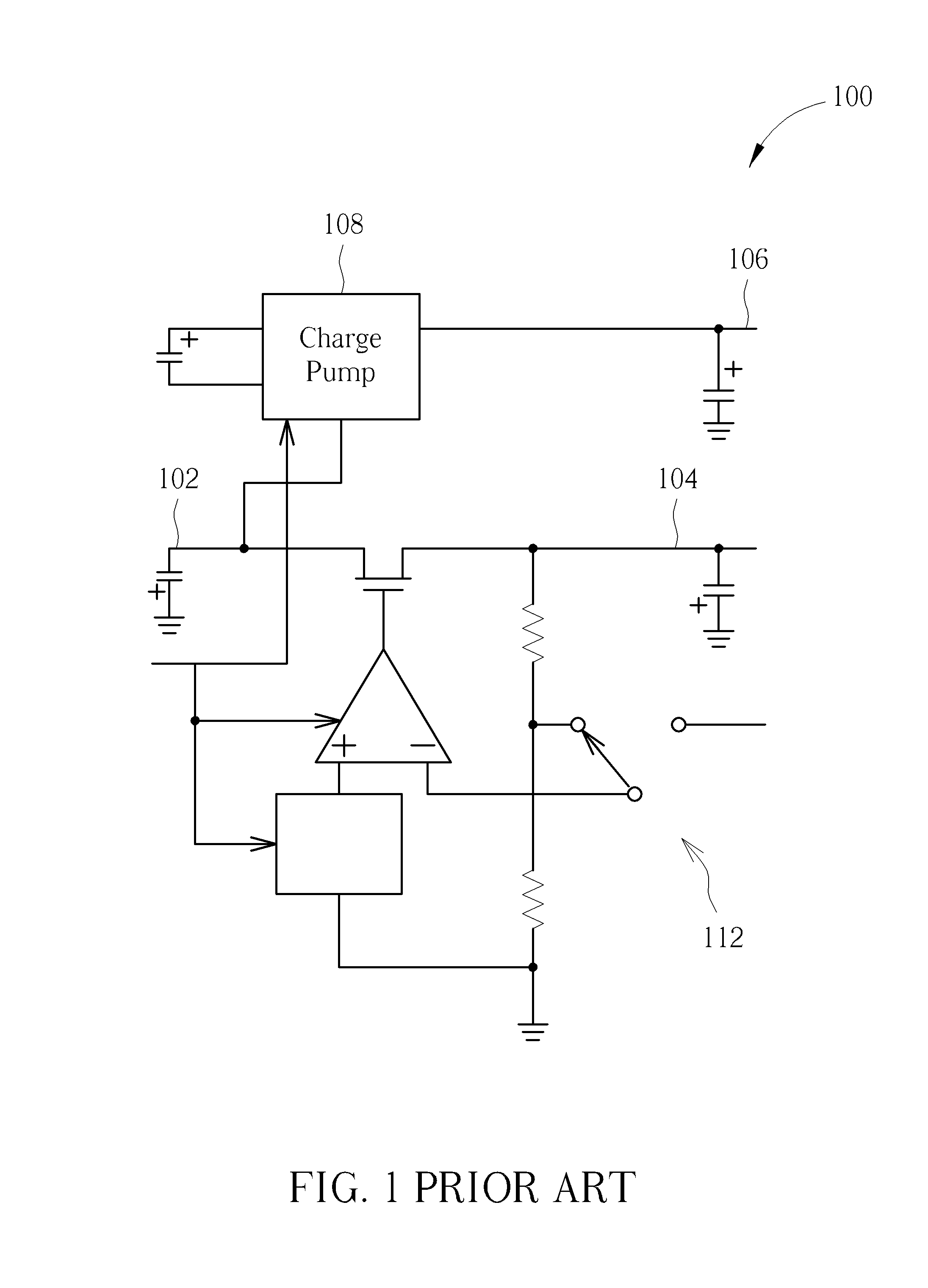
This has the disadvantage of increasing the current supplied by the negative supply, reducing overall efficiency and increasing the levels of the spurs associated with the negative voltage generation.

Method used


Image

  • Charge pump circuit, integrated circuit, electronic device and method therefor
  • Charge pump circuit, integrated circuit, electronic device and method therefor
  • Charge pump circuit, integrated circuit, electronic device and method therefor

Examples


Embodiment Construction

[0032]Examples of the invention are described with reference to a circuit that includes spurious filtering but where the filter is now included within the regulation control loop. Examples of the invention will be described in terms of a circuit that generates a negative voltage. Examples of the invention will also be described in terms of some auxiliary circuits around it and / or enhanced embodiments, such as level shifting. Examples of the invention will also be described in terms of output voltage that is programmable, whereby the circuit includes filtering to minimise spurious emissions, particularly at RF frequencies, along with measures to improve start-up time.

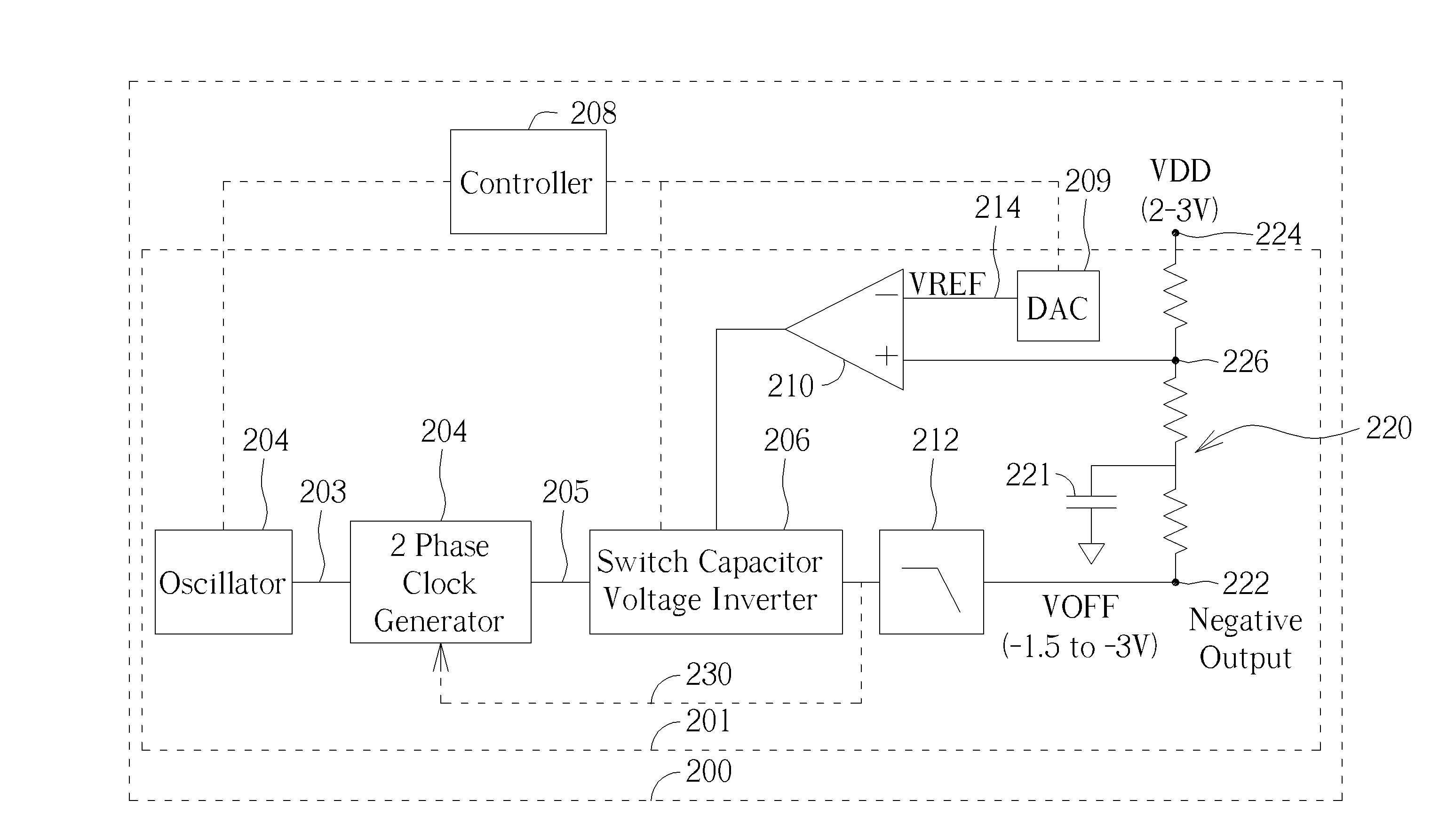
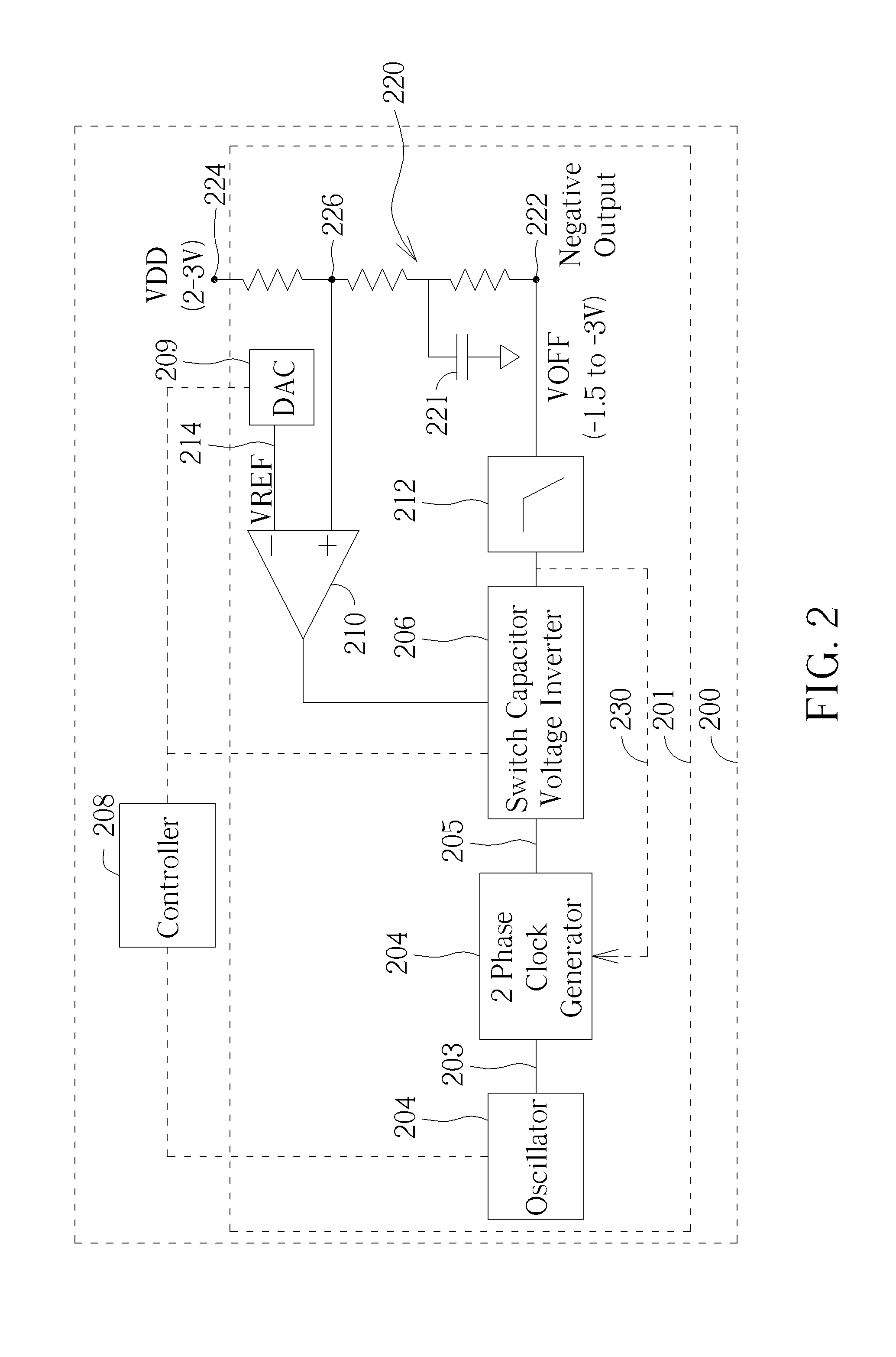
[0033]Referring to FIG. 2, a detailed example of an electronic device 200 is illustrated, according to some examples of the invention. In this example, the electronic device 200 may comprise an integrated circuit 201, which may be suitable for a (high-power) RF switching circuit. In this example, the electronic device 20...


PUM


Abstract

A charge pump circuit for generating a negative voltage has: a clock generator arranged to output at least one clock signal; a switched capacitor voltage inverter circuit including capacitive elements wherein the switched capacitor voltage inverter circuit receives the at least one clock signal and generates a negative voltage therefrom. The charge pump circuit further has a regulation control loop providing a feedback path from an output of the switched capacitor voltage inverter circuit to a supply input of the switched capacitor voltage inverter circuit, and an output arranged to output a generated negative voltage. The feedback path has an operational amplifier configured to generate a maximum charging supply voltage from a fed back level-shifted negative voltage and apply the maximum charging supply voltage to the input supply of the switched capacitor voltage inverter to charge at least one of the capacitive elements during a loop start up.

Description

CROSS REFERENCE TO RELATED APPLICATIONS[0001]This application claims the benefit of U.S. provisional application No. 62 / 072,437, filed on Oct. 30, 2014 and incorporated herein by reference.BACKGROUND[0002]1. Field of the Invention[0003]The field of this invention relates to a charge pump circuit, an integrated circuit for a charge pump, an electronic device and a method therefor. In particular, the field of the invention may relate to negative voltage generation circuits employing charge pumps to switch off transistor devices.[0004]2. Background of the Invention[0005]In the field of radio frequency (RF) switches, such as RF silicon-on-insulator (SOI) switches, generally a negative voltage is required in order to disable (turn ‘off’) the SOI switches under a large RF swing. The generation of a negative voltage allows the RF switch designer to avoid the use of DC blocking capacitors. Such a negative voltage is commonly generated by utilising a charge pump circuit, which requires an os...

Claims


Application Information

Patent Timeline
IPC IPC(8): H02M3/07
CPCH02M3/07H02M1/36H02M3/071
Inventor FOWERS, PAULCOLLADOS ASENSIO, MANEL
Owner MEDIATEK SINGAPORE PTE LTD SINGAPORE
Learn More