On-chip ESD protection circuit for radio frequency (RF) integrated circuits

a protection circuit and integrated circuit technology, applied in the field of esd, can solve the problems of infancy of esd protection circuitry for newer technologies, the potential for destructive esd events has become more serious, and products, typically handheld devices, are much more prone to esd-induced damage, etc., to achieve low parasitic capacitance, low impedance path, and low on-state resistance

Inactive Publication Date: 2009-09-22
QORVO US INC
View PDF7 Cites 60 Cited by
  • Summary
  • Abstract
  • Description
  • Claims
  • Application Information

AI Technical Summary

Benefits of technology

[0018]An electrostatic discharge (ESD) protection circuit between a signal path and ground is described. A trigger sub-circuit detects a voltage on the signal path above a defined threshold and activates a main protection sub-circuit, which provides a discharge path to ground while the voltage signal remains above the threshold. The main protection sub-circuit avoids the use of an extended diode stack by employing a depletion-mode (D-mode) field effect transistor (FET) in series with a diode pair for the discharge path. The diode pair in the discharge path biases the transistor off during normal operation. The ESD protection circuit exhibits low on-state resistance and low parasitic capacitance when compared with conventional ESD protection circuits. The parasitic resistance of the diode pair along with the on resistance of the FET (Rdson) are sufficiently low to provide a low impedance path for the ESD pulse.

Problems solved by technology

Electrostatic discharge (ESD), which is a large subset of electrical overstress (EOS), is a major reliability issue in integrated circuits (ICs).
As semiconductor devices have scaled to smaller dimensions and ICs have become more complex, the potential for destructive ESD events has become more serious.
More recently, there has been a tremendous demand for increasing the ESD robustness of Radio Frequency Integrated Circuits (RFICs) especially for wireless applications, since such products, typically handheld devices, are much more prone to ESD-induced damages.
However, ESD protection circuitry for newer technologies is still in its infancy.
However, ESD protection circuitry for GaAs pHEMT technology that is currently in use provides undesirable characteristics.
However, current GaAs pHEMT ESD protection structures have unwanted parasitic capacitances and resistances which may adversely affect performance of radio frequencies (RF) circuits.
In particular, at RF frequencies, the parasitics associated with the ESD structures can lead to impedance mismatches.
Impedance mismatches can cause signal reflection which degrades the performance of the circuit which it is intended to be protected.
Additionally, a protection circuit, such as that shown in FIG. 1, is unsuitable for pHEMT switches.
The use of large diode stacks for ESD protection circuitry also increases diode size.
This increase in diode size correlates to an increase in cost of manufacturing and, thereby, cost to consumers.
Another issue with the use of diode stacks is associated with the on-state resistance of the stack.
However, though paralleling several diode stacks improves the on-state resistance of the ESD protection circuit, it has two additional problems associated with it.
First, by paralleling redundant stacks of diodes, the area required for the ESD protection circuitry increases dramatically.
Second, because each diode has a parasitic capacitance associated with it as well, the parasitic capacitance of the ESD protection circuit increases as the number of diode stacks that are paralleled increases.
This increase in parasitic capacitance negatively affects circuit performance, as described above.

Method used


Image

  • On-chip ESD protection circuit for radio frequency (RF) integrated circuits
  • On-chip ESD protection circuit for radio frequency (RF) integrated circuits
  • On-chip ESD protection circuit for radio frequency (RF) integrated circuits

Examples


Embodiment Construction

[0028]The embodiments set forth below represent the necessary information to enable those skilled in the art to practice the invention and illustrate the best mode of practicing the invention. Upon reading the following description in light of the accompanying drawing figures, those skilled in the art will understand the concepts of the invention and will recognize applications of these concepts not particularly addressed herein. It should be understood that these concepts and applications fall within the scope of the disclosure and the accompanying claims.

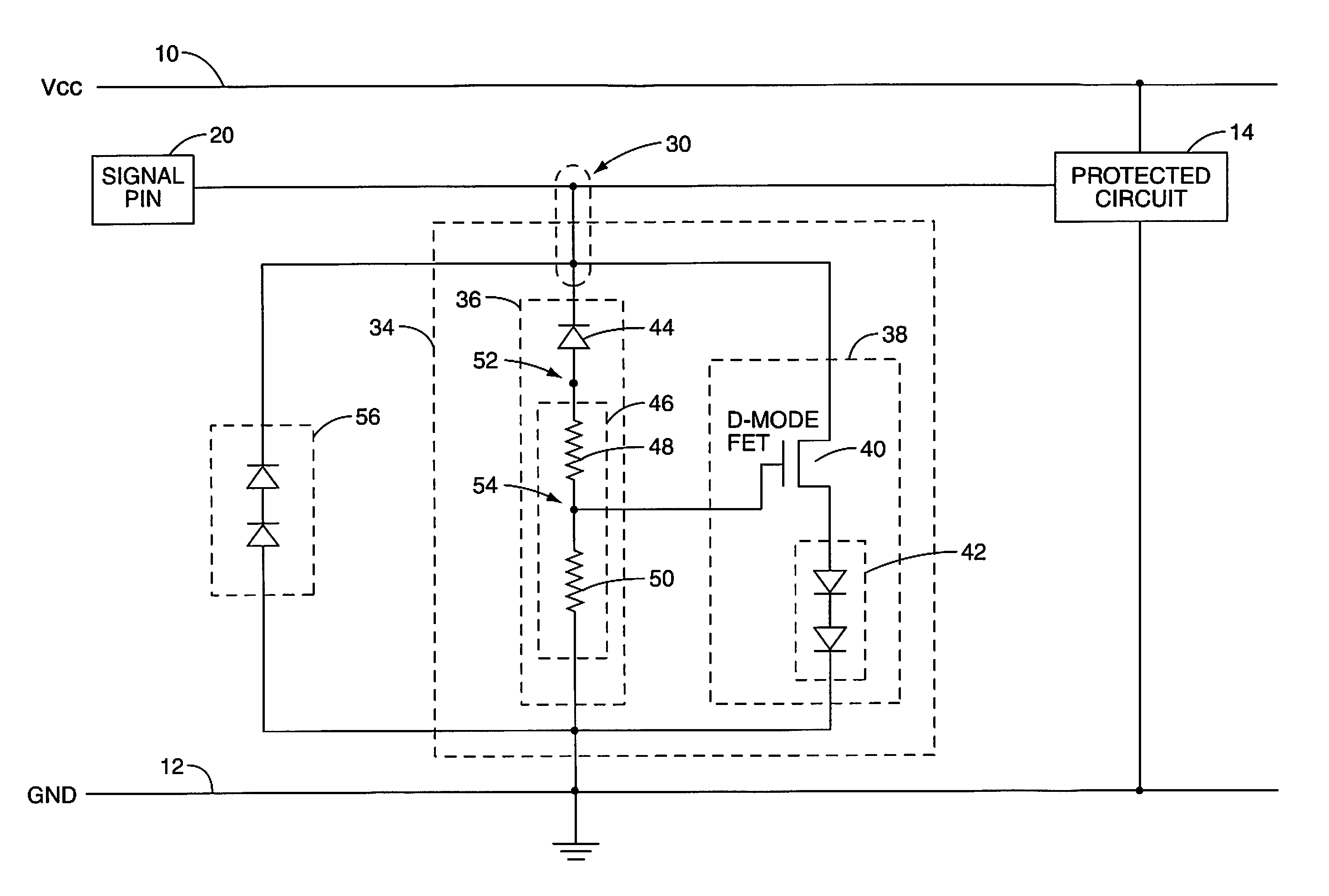
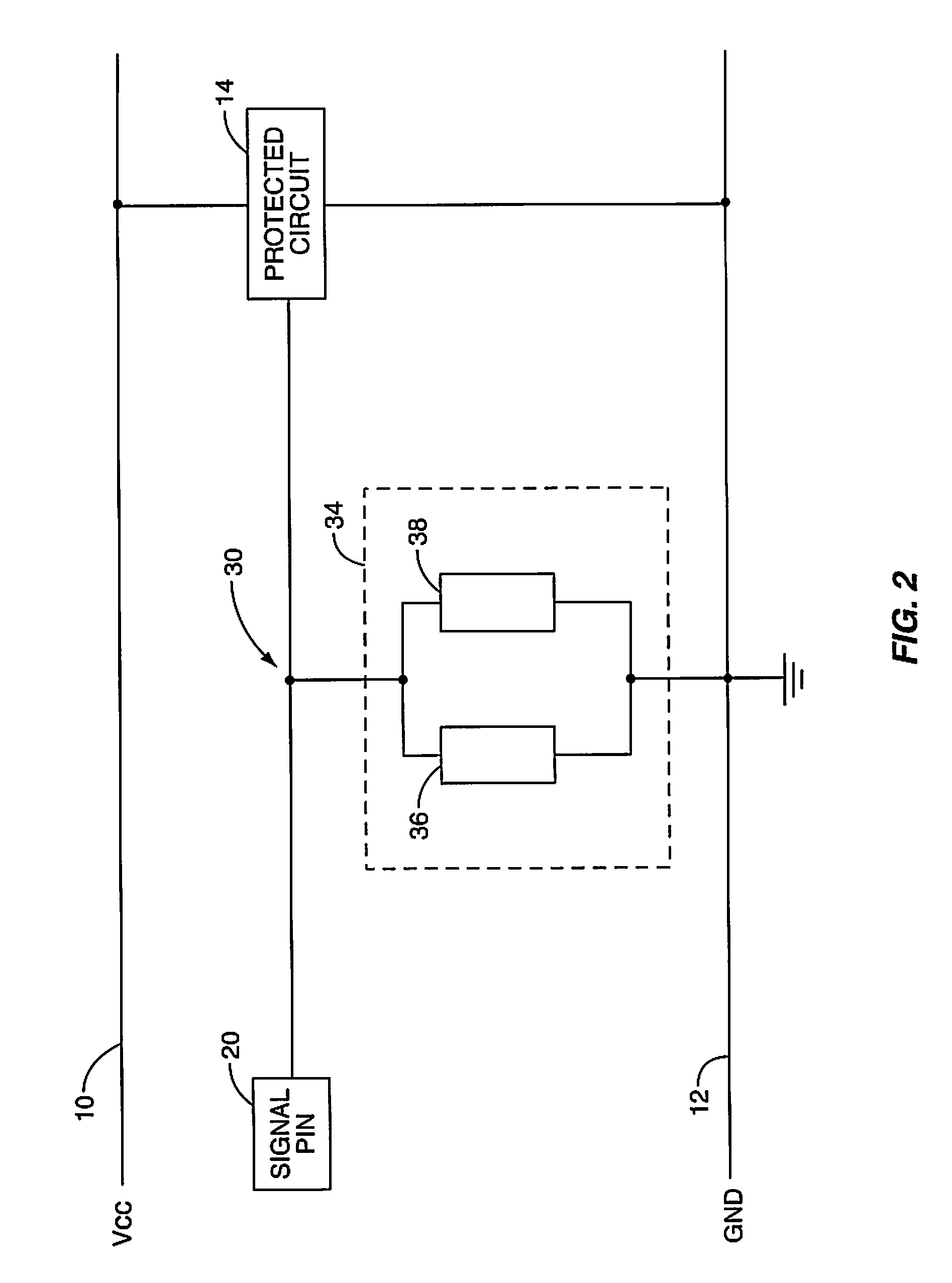
[0029]FIG. 2 illustrates an electrostatic discharge (ESD) protection circuit according an embodiment of the present invention, including a trigger sub-circuit and a main protection sub-circuit. An ESD protection circuit 34 is illustrated including a trigger sub-circuit 36 and a main protection sub-circuit 38. The trigger sub-circuit-circuit 36 will detect ESD surge events and trigger the main protection sub-circuit-circuit 38. The...


PUM


Abstract

Methods and apparatus for ESD protection of pseudomorphic high electron mobility transistor (pHEMT) circuitry are described. In one method, an ESD surge is detected at a trigger circuit. An ESD protection circuit is triggered. Current flow within the trigger circuit is limited and ESD energy is dispersed to a ground plane via the ESD protection circuit.

Description

RELATED APPLICATIONS[0001]This application claims the benefit of U.S. Provisional Patent Application Ser. No. 60 / 811,255, which was filed in the U.S. Patent and Trademark Office on Jun. 6, 2006, which is incorporated herein by reference.FIELD OF THE INVENTION[0002]The subject matter described herein relates to electrostatic discharge (ESD) protection circuitry. More particularly, an ESD protection circuit for radio frequency (RF) integrated circuits that exhibits a low on-state resistance and low parasitic capacitance is described.BACKGROUND OF THE INVENTION[0003]Electrostatic discharge (ESD), which is a large subset of electrical overstress (EOS), is a major reliability issue in integrated circuits (ICs). EOS and ESD together account for more than 60% of failures in ICs. As semiconductor devices have scaled to smaller dimensions and ICs have become more complex, the potential for destructive ESD events has become more serious.[0004]More recently, there has been a tremendous demand ...

Claims


Application Information

Patent Timeline
Patent Type & Authority Patents(United States)
IPC IPC(8): H02H9/00H02H1/00
CPCH02H9/046
Inventor IVERSEN, CHRISTIAN RYEMUTHUKRISHNAN, SWAMINATHANPEACHEY, NATHANIEL
Owner QORVO US INC
Why Eureka
Try Eureka