

High-density electronic package and method for making same
A technology of electronic packaging and electronic devices, applied in the field of electronic device packaging
- Summary
- Abstract
- Description
- Claims
- Application Information
AI Technical Summary
Problems solved by technology
Method used
Image

Examples
Embodiment Construction
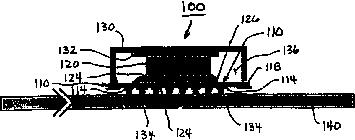
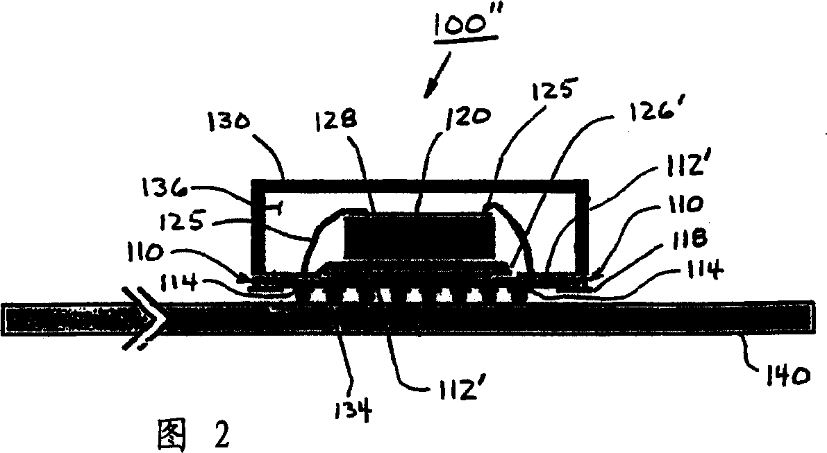
[0031] Electronic packaging is subject to heat-induced forces and moisture sealing. Each device package consists of a semiconductor chip or die, which is attached to an intermediate stack substrate, such as an FR4 stack, by die glue. Fine gold or aluminum bond wires connect the connection terminals of the semiconductor chip to corresponding conductors on the substrate, which is connected to the underlying substrate by a connection that may be a solder or conductive adhesive conductor. Semiconductor chips and bond wires are typically encapsulated with a molded encapsulant or covered with a cover that provides mechanical support and moisture barrier.
[0032] Mechanical stresses arise due to differences in coefficient of thermal expansion (CTE) and high modulus of elasticity (ME), ie stiffness, of the different materials used in such modules. The silicon semiconductor die has a CTE of about 3 ppm / °C, the adhesive has a CTE of about 40 ppm / °C, the substrate has a CTE of about 1...
PUM
 Abstract
Description
Claims
Application Information