

Semi-conductor device
A semiconductor and conductive layer technology, applied in semiconductor devices, semiconductor/solid-state device manufacturing, semiconductor/solid-state device components, etc., can solve problems such as the inability to obtain electromagnetic wave shielding effects, achieve good electromagnetic wave shielding effects, and prevent the reduction of magnetic force line density , The effect of suppressing the reduction of the magnetic line density
- Summary
- Abstract
- Description
- Claims
- Application Information
AI Technical Summary
Problems solved by technology
Method used
Image

Examples
no. 1 approach
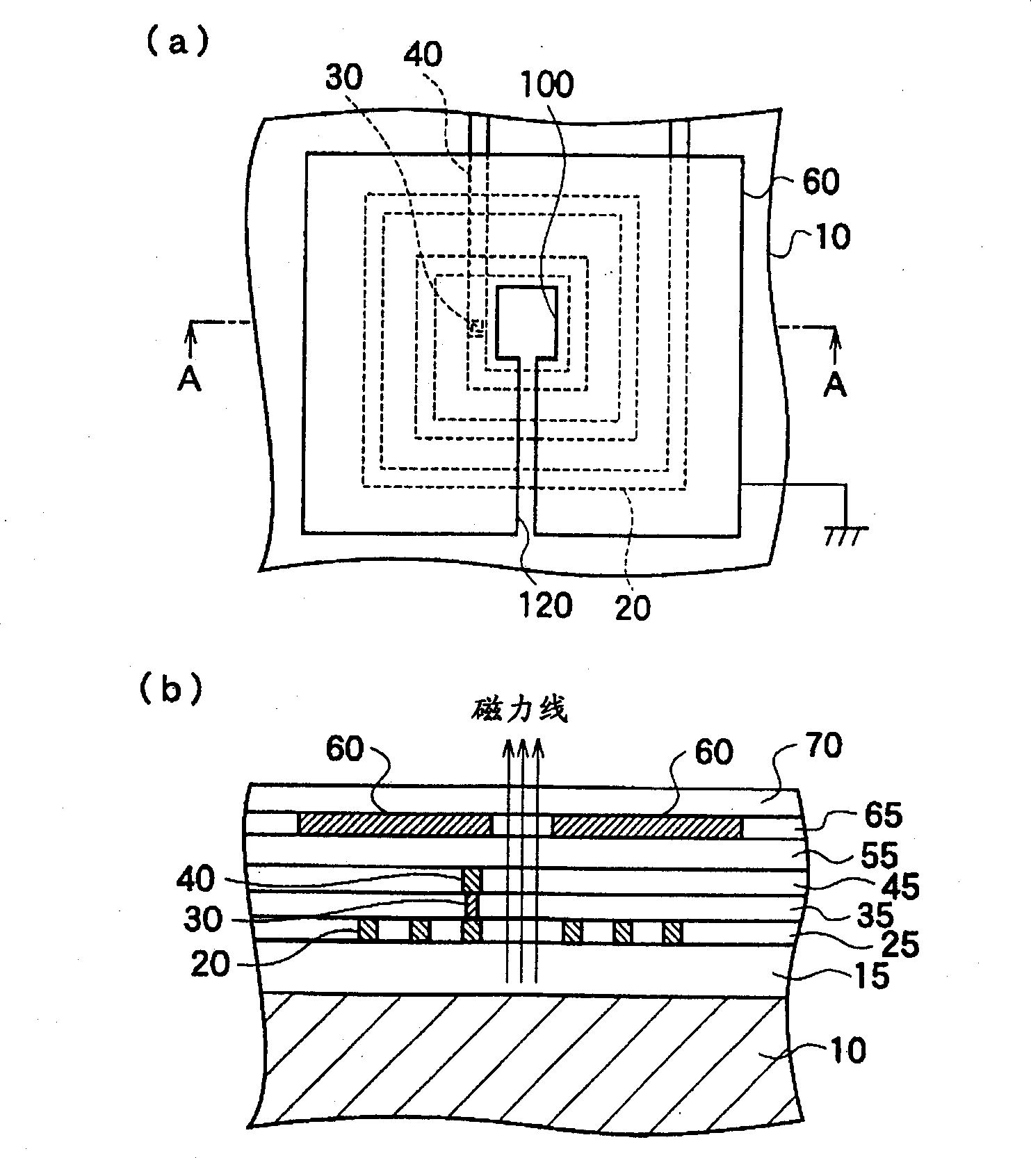
[0029] figure 1 (a) is a front view showing a first embodiment of the semiconductor device of the present invention; figure 1 (b) is figure 1 Sectional view at dashed line A-A in (a).
[0030] Such as figure 1 As shown in (a), the semiconductor device according to the first embodiment has a spiral inductor 20 having a spiral pattern formed in the same plane, and an electromagnetic wave shielding layer 60 . The electromagnetic wave shielding layer 60 has an opening 100 in a region corresponding to the region surrounded by the innermost circle of the spiral inductor 20 , and has a slit 120 extending from the opening to the peripheral portion of the electromagnetic wave shielding layer 60 .
[0031] Next, the configuration of each part will be described more specifically.
[0032] There is no particular restriction on the formation position of the spiral inductor, but it can be as figure 1 As shown in (b), for example, the same layer is formed at the position of the fir...
no. 2 approach
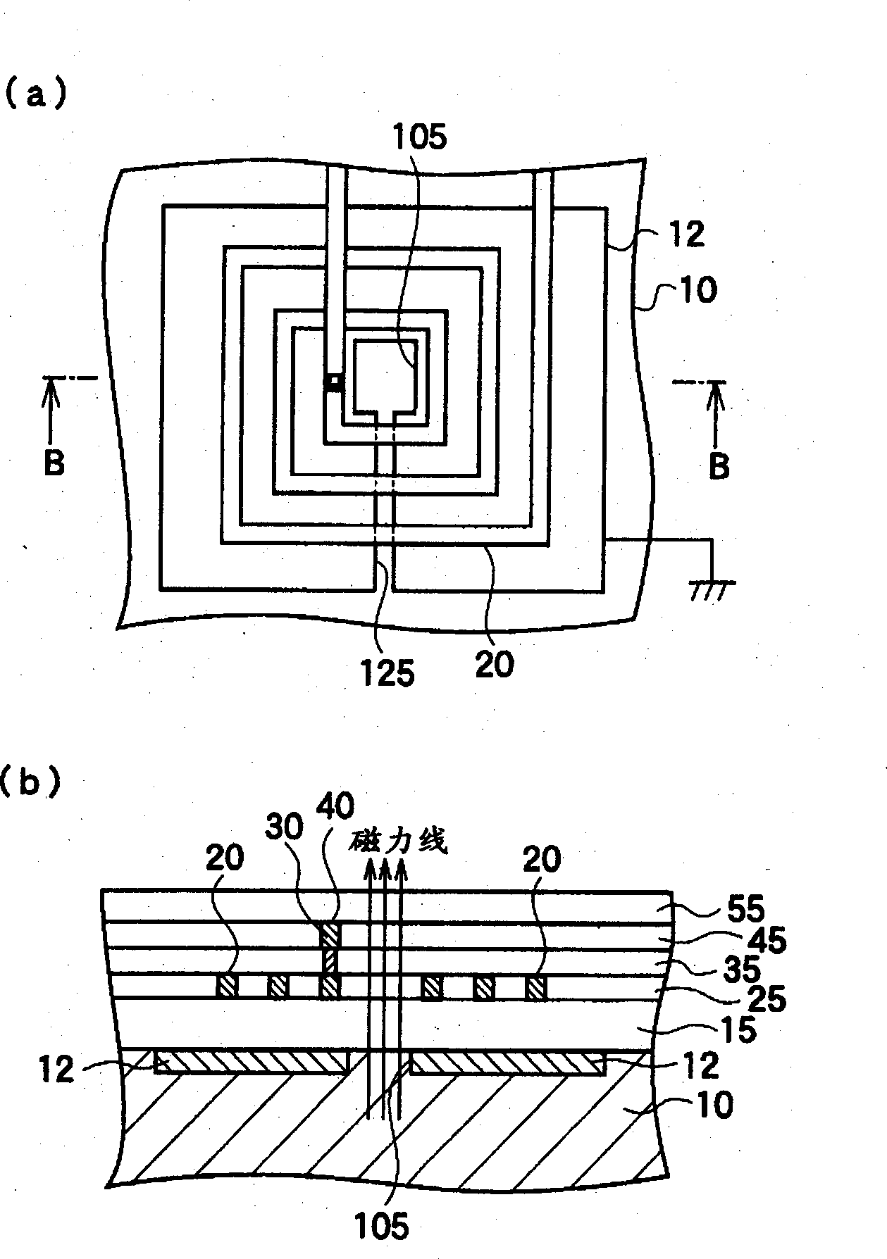
[0049] figure 2 (a) is a front view showing a second embodiment of the semiconductor device of the present invention; figure 2 (b) is figure 2 Sectional view at the dashed line B-B in (a).
[0050] As in the first embodiment, also in the second embodiment, the electromagnetic wave shielding layer has an opening in a region corresponding to the region surrounded by the innermost circle of the spiral inductor, and has openings extending from the opening to the A gap in the peripheral portion of the electromagnetic wave shielding layer. However, it is different from the first embodiment in that the electromagnetic wave shielding layer is formed under the spiral inductor.
[0051] Such as figure 2 As shown in (a) and 2(b), similarly to the first embodiment, the first wiring layer on the first interlayer insulating film 15 formed on the semiconductor substrate 10 is patterned to form a spiral pattern having a spiral shape. Figure 20 of the spiral inductor. The size and sh...
no. 3 approach
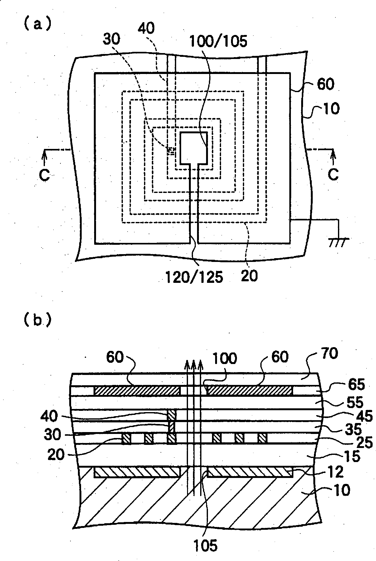
[0057] image 3 (a) is a front view showing a third embodiment of the semiconductor device of the present invention; image 3 (b) is image 3 Sectional view at dashed line C-C in (a).
[0058] Like the first and second embodiments, in the third embodiment, the electromagnetic wave shielding layer has an opening in a region corresponding to the region surrounded by the innermost circle of the spiral inductor, and has openings from the opening. A slit extending to the peripheral portion of the electromagnetic wave shielding layer. However, the electromagnetic wave shielding layer is formed above and below the spiral inductor, which is different from the first and second embodiments.
[0059] Such as image 3 As shown in (a) and 3(b), similarly to the first and second embodiments, the first wiring layer on the first interlayer insulating film 15 formed on the semiconductor substrate 10 is formed to have a spiral shape. The spiral inductor 20 of the spiral pattern. The size ...
PUM
 Abstract
Description
Claims
Application Information