
Semiconductor device and its manufacturing method

A technology of semiconductors and devices, which is applied in the field of semiconductor devices and the manufacture of such devices, and can solve problems such as unsatisfactory matching properties of DRAM cells

Inactive Publication Date: 2003-03-05
SONY CORP
View PDF0 Cites 11 Cited by
  • Summary
  • Abstract
  • Description
  • Claims
  • Application Information

AI Technical Summary

Problems solved by technology

Therefore, the manufacturing process of the above-mentioned replacement gate makes the matching properties with the stacked DRAM cells unsatisfactory

Method used


Image

  • Semiconductor device and its manufacturing method
  • Semiconductor device and its manufacturing method
  • Semiconductor device and its manufacturing method

Examples


Embodiment Construction

[0030] Detailed description of the preferred embodiment

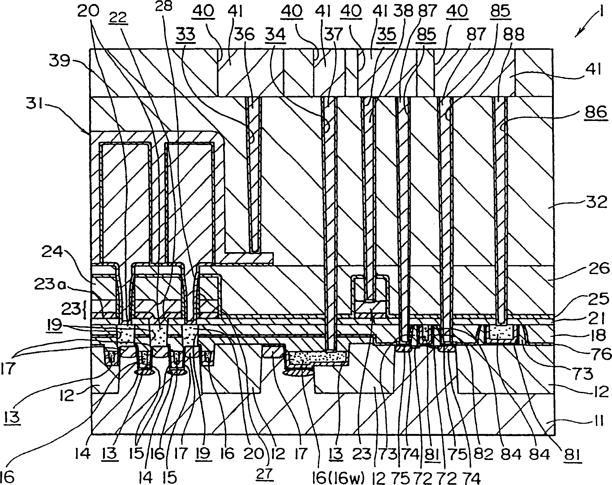
[0031] Referring now to the schematic cross-sectional view showing the structure of the device figure 1 An example of an embodiment of the semiconductor device according to the present invention will be described.

[0032] Such as figure 1 As shown, an element isolation region 12 is formed on a semiconductor substrate 11 .

[0033] STI (Shallow Trench Isolation) technology is used to make the element isolation region with a depth of 0.1-0.2 microns (μm). Grooves 13 having a depth of approximately 50 to 100 nanometers (nm) are formed on the semiconductor substrate 11 and the element separation region 12 . In the trench 13, a word line (gate electrode) 16 passing through the gate insulating film 15 is formed. Even if there is a difference between the depth of the groove 13 formed on the semiconductor substrate 11 and the depth of the groove 13 formed on the element separation region 12, there will be no problem.

[0...


PUM


Abstract

The present invention provides a DRAM in which junction leak is suppressed without increasing capacity of a capacitor and a contact area between a diffusion layer and a take-out electrode is increased to decrease contact resistance between them, whereby small-sizing of the DRAM cell can be achieved and an insulating withstand voltage across a gate electrode and the take-out electrode can be secured. In a semiconductor device having a memory element and a logic element formed on the same semiconductor substrate, a transistor of the memory element comprises a gate electrode (16) embedded within a trench (13) formed in a semiconductor substrate (11) through a gate insulating film (15) and a diffusion layer (17) formed on the side of the semiconductor substrate (11) at a side wall of the trench (13), and a take-out electrode (20) connected to the diffusion layer (17) is provided so that the take-out electrode overlaps the gate electrode (16) through a first interlayer insulating film (insulating film) (18) on the gate electrode (16). A word line (16) is also provided in the trench (13) and an impurity concentration of the diffusion layer (17) is decreased as a depth thereof is increased.

Description

technical field [0001] The present invention relates to a semiconductor device and a method of manufacturing the device; more particularly, to a semiconductor device in which DRAM (Dynamic Random Access Memory) and logic elements are mixedly manufactured on the device and a method of manufacturing the device. Background technique [0002] Semiconductor manufacturers compete each year to rapidly develop micro-manufacturing processes. The manufacture of semiconductor devices strives to develop a complex device whose DRAM has a large capacity, and logic elements that can be driven at high speed, both of which are fabricated on one chip. As an example of such a device, gates of memory cells of a DRAM are arranged on a substrate such that the gates are stacked on top of each other. In order to remove the diffusion layer of the memory cell transistors, so-called self-alignment contacts are introduced, while logic components do not use self-alignment contacts. [0003] However, i...

Claims


Application Information

Patent Timeline
Patent Type & Authority Applications(China)
IPC IPC(8): H01L27/092H01L21/8238H01L21/8242H01L27/108
CPCH01L27/10876H01L27/10891H01L27/10855H01L27/10894H01L27/10814H10B12/315H10B12/0335H10B12/053H10B12/488H10B12/09H10B12/00
Inventor 梅林拓
Owner SONY CORP
Learn More