Semi-conductor storage device
A storage device and semiconductor technology, which is applied in semiconductor devices, semiconductor/solid-state device manufacturing, static memory, etc., can solve the problems of increasing chip area, increasing data lines, increasing manufacturing costs, etc.
- Summary
- Abstract
- Description
- Claims
- Application Information
AI Technical Summary
Problems solved by technology
Method used
Image

Examples
Embodiment Construction
[0047] Hereinafter, embodiments of the present invention will be described in detail with reference to the drawings.
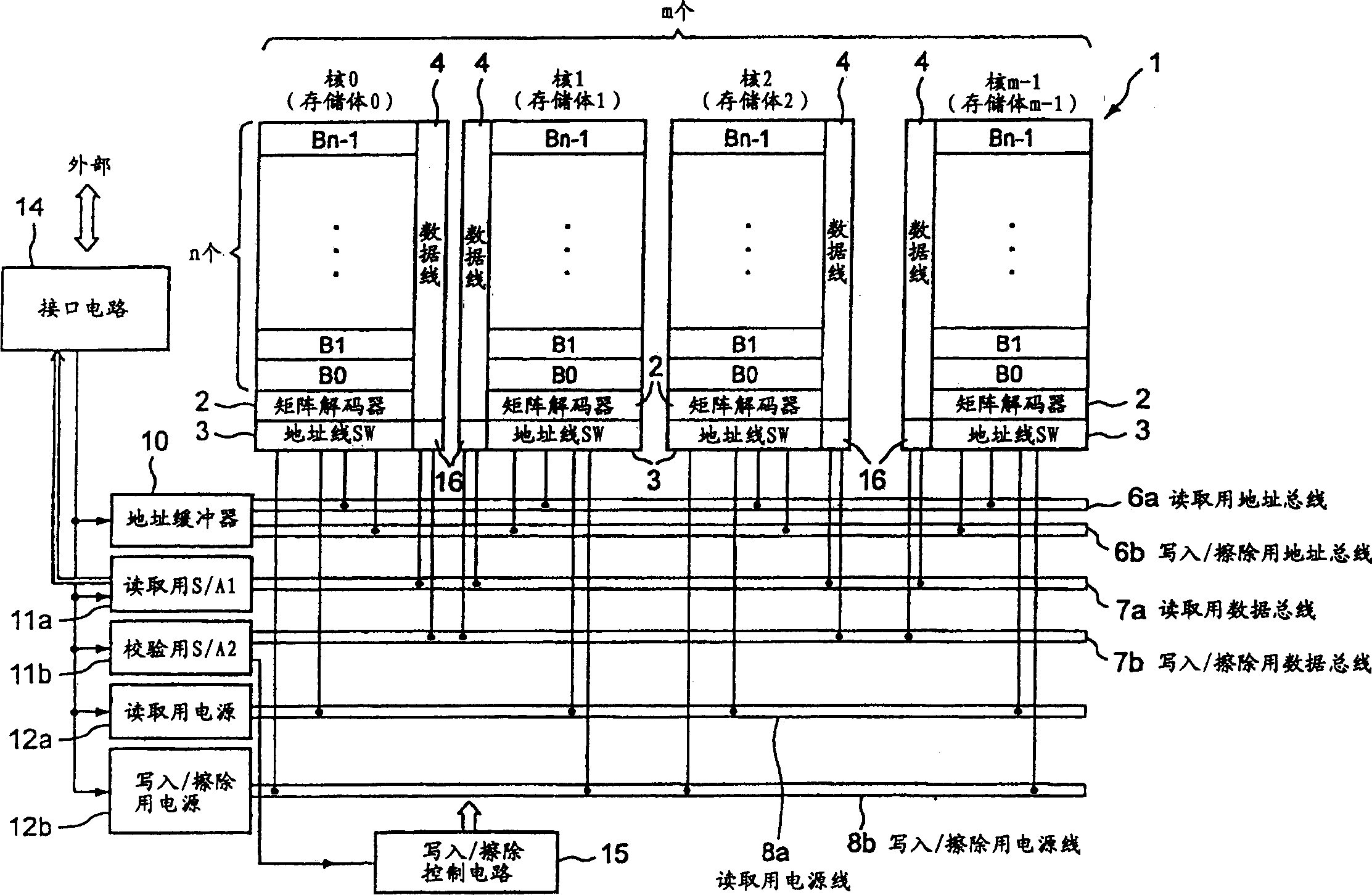
[0048] figure 1 It shows an example of the chip structure of a simultaneously realizable flash memory disclosed in the above-mentioned Japanese Patent Application No. 2000-127106 as a semiconductor memory device to which the present invention is applied.
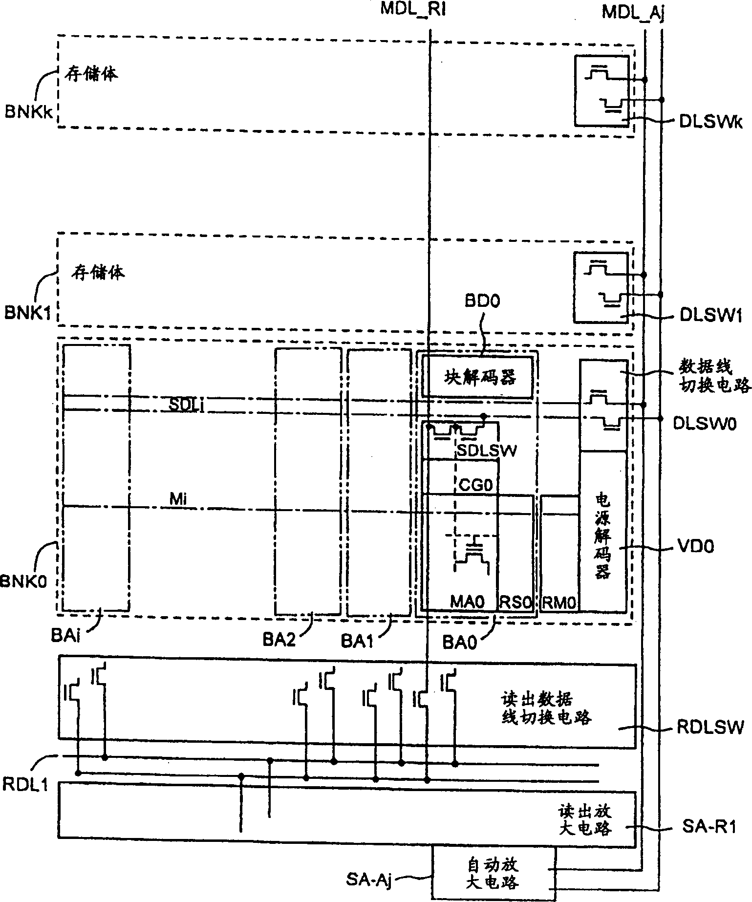
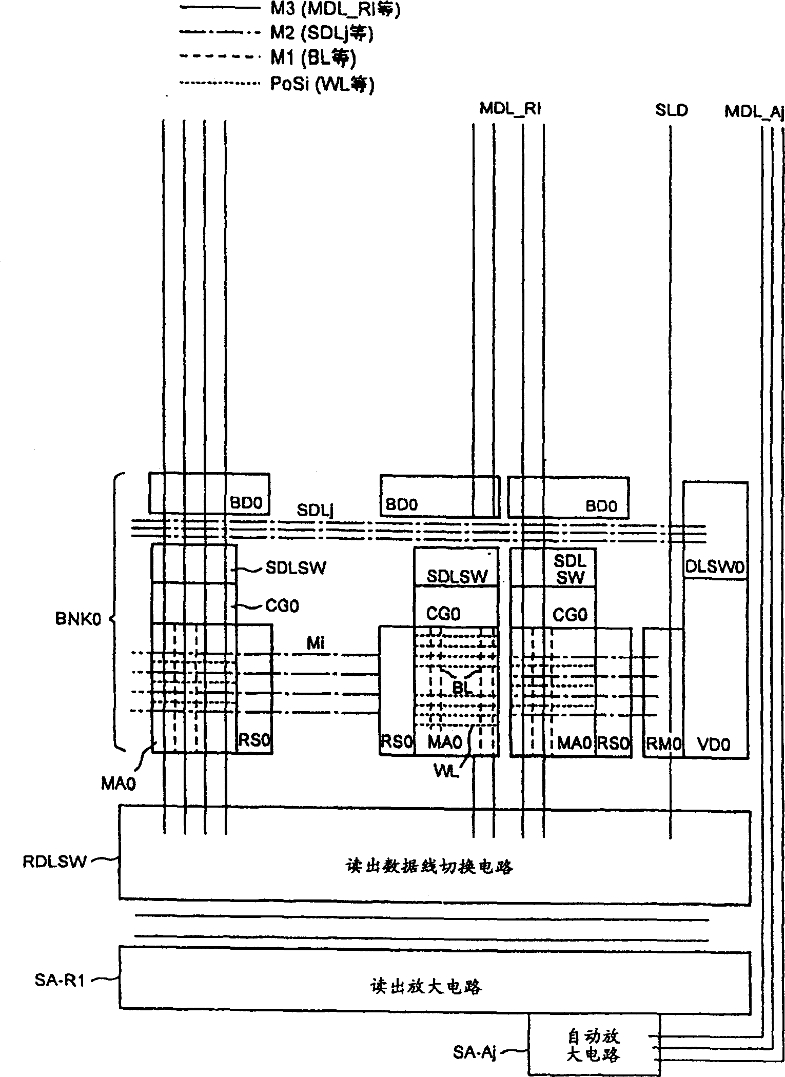
[0049] exist figure 1 Among them, the memory cell array 1 is composed of m cores (core) 0 to m-1 formed by arranging n blocks B0 to Bn-1 respectively. Each block B0 to Bn-1 is the smallest unit of data erasing, and is arranged in a plurality of memory cells. The memory cell is, for example, a nonvolatile memory cell with a stacked gate structure. A core is defined as a set of one or more blocks, but in the example in the figure, one bank is formed by every n blocks B0 to Bn−1.
[0050] In each core, a matrix decoder 2 including a row decoder and a column decoder for selecting a memory cell, a switch ci...
PUM
 Abstract
Description
Claims
Application Information
 - R&D
- Intellectual Property
- Life Sciences
- Materials
- Tech Scout
- Unparalleled Data Quality
- Higher Quality Content
- 60% Fewer Hallucinations
Browse by: Latest US Patents, China's latest patents, Technical Efficacy Thesaurus, Application Domain, Technology Topic, Popular Technical Reports.
© 2025 PatSnap. All rights reserved.Legal|Privacy policy|Modern Slavery Act Transparency Statement|Sitemap|About US| Contact US: help@patsnap.com