Organic film transistor and preparing method

An organic thin film and transistor technology, which is applied in the field of the preparation of structured organic thin film transistors, can solve the problems of poor insulation performance of high dielectric materials, increase leakage current, etc., so as to increase channel capacitance, reduce turn-on voltage, and reduce adverse effects. Effect

Inactive Publication Date: 2003-04-09
CHANGCHUN FULEBO DISPLAY TECH
View PDF1 Cites 28 Cited by
  • Summary
  • Abstract
  • Description
  • Claims
  • Application Information

AI Technical Summary

Problems solved by technology

Unfortunately, both methods increase the leakage current between the gate-source and gate-drain electrodes of the device, mainly due to the poor insulation performance of high-dielectric materials

Method used


Image

  • Organic film transistor and preparing method
  • Organic film transistor and preparing method
  • Organic film transistor and preparing method

Examples


Embodiment 1

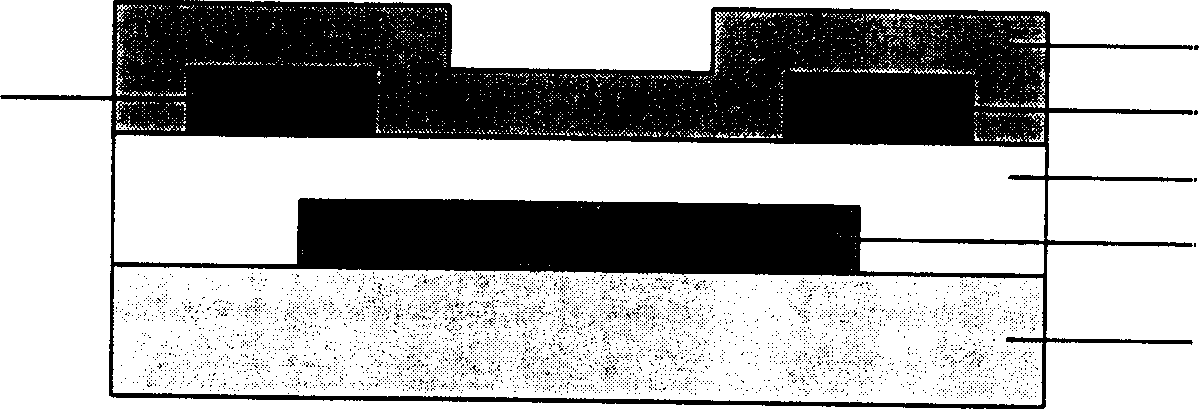
[0022] As shown in Figure 6, on the 7059 glass substrate 1, a layer of Ta metal film is plated on the 7059 glass substrate by the radio frequency magnetron sputtering method (the condition of sputtering is: background vacuum 2 × 10 -3 Pa; Ar gas pressure 1Pa; radio frequency power 500W; substrate temperature 100 degrees) and photolithography into the gate shape 2. A layer of 400 nm Ta was continuously sputtered by DC magnetron sputtering on the gate. 2 o 5 and a layer of 300 nm SiO 2 (reactive sputtering: background vacuum 2×10 -3 Pa; O 2 Air pressure 0.9Pa; DC power 500W; substrate temperature 100 degrees) as the gate insulating layer 3 and the second insulating layer 4 respectively. Then apply photoresist, expose, develop, and then use the photoresist as a drain plate in 10 -5 A layer of 100 nanometer gold (Au) is thermally evaporated under a high vacuum of Pa, and the sample is put into an acetone solvent to peel off the gold in the non-patterned area to form the sourc...

Embodiment 2

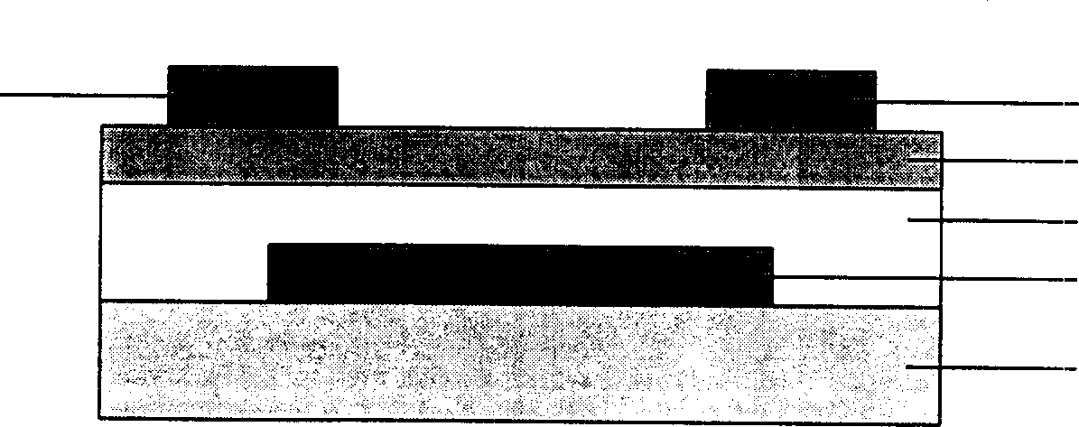
[0024] As shown in Figure 6, a layer of MoW alloy film is plated on the flexible plastic substrate 1 by radio frequency magnetron sputtering (the sputtering method is co-sputtering of Mo target and W target, and the condition of sputtering is: background vacuum 2×10 -3 Pa; Ar gas pressure 1Pa; radio frequency power 500W; substrate temperature 100 degrees) and photolithography into the gate shape 2. A layer of 500 nm Ta was sputtered on the grid by DC magnetron sputtering 2 o 5 (reactive sputtering: background vacuum 2×10 -3 Pa; O 2 air pressure 0.9Pa; DC power 500W; substrate temperature 100 degrees) as the gate insulating layer 3 , and then a layer of 300nm polymethyl methacrylate (PMMA) was spin-coated as the second insulating layer 4 . Next, apply photoresist, expose, develop, and then use the photoresist as a drain plate in 10 -5 A layer of silver (Ag) of 100 nanometers is thermally evaporated under a high vacuum of Pa, and the sample is put into an acetone solvent to...

Embodiment 3

[0026] As shown in Figure 6, a layer of chromium metal film is plated on the flexible plastic substrate 1 by radio frequency magnetron sputtering (the sputtering method is chromium target sputtering, and the sputtering condition is: background vacuum 2 × 10 -3 Pa; Ar gas pressure 1Pa; radio frequency power 500W; substrate temperature 100 degrees) and photolithography into the gate shape 2. A layer of 500nm TiO was sputtered on the grid by DC magnetron sputtering 2 (reactive sputtering: background vacuum 2×10 -3 Pa; O 2 air pressure 0.9Pa; DC power 500W; substrate temperature 150 degrees) as the gate insulating layer 3 , and then a layer of 300nm polyimide was spin-coated as the second insulating layer 4 . Next at 10 -5 A layer of 100 nanometer aluminum (AL) is thermally evaporated under a high vacuum of Pa, and then coated with photoresist, exposed, developed, and then photoetched to form a source electrode 5 and a drain electrode 6 . The channel width is 1000 microns, and...


PUM


Abstract

An organic film transistor includes a substrate with a grid on it, a grid insulation layer on the grid, a source / drain on the insulation layer and a semiconductor active layer formed on the source / drain, among which the insulation layer comprises a first and a second insulation layers with different dielectric constants. By only adding spin coating or evaporation coating of the second insulation film and self-aligned dry etching, this invention can improve the injection characteristics of carriers not adding photoetching of the regular complicated technology so as to increase OTFT performance, and also the block the drain leakage current of the grating insulation film and reduce the parasitic capacitance, thus high dielectric material can be applied to the grating insulation layer to increase channel capacitance to reduce the starting voltage.

Description

technical field [0001] The present invention relates to an organic thin film transistor (hereinafter referred to as OTFT). The invention also relates to the preparation method of the organic thin film transistor with this structure. Background technique [0002] In recent years, the performance of OTFT has been continuously improved, and the room-temperature carrier field-effect mobility of transistor devices of some organic materials (such as Pentacene, Oligothiophene, Tetracene, etc.) has exceeded 1 (square centimeter per volt per second). Active matrix displays and flexible integrated circuits show application potential. Due to the sensitivity of organic semiconductors to solvents in conventional photolithography processes, microfabrication of devices is generally difficult. Therefore, at present people generally adopt the method that the organic semiconductor layer is placed on the source-drain electrode (generally called the bottom electrode configuration OTFT, accomp...

Claims


Application Information

Patent Timeline
Patent Type & Authority Applications(China)
IPC IPC(8): H01L21/02H01L21/316H01L29/76H01L35/24H01L47/00H01L51/00H01L51/30
CPCH01L21/31691H01L51/0078H01L51/0516H01L28/56H01L51/0545H01L21/31604H10K85/311H10K10/468H10K10/466H01L21/02263H01L21/02197H10K10/474
Inventor 阎东航袁剑峰
Owner CHANGCHUN FULEBO DISPLAY TECH
Why Eureka
Try Eureka